 deʃhipu
Apparently some fab houses can do firmware programming and testing of the devices right in the factory — you just have to provide detailed step-by-step instructions on how to do it. So I started work on the firmware flashing guide and on the test program. I also modified the version 8 PCB design that I have on order from Aisler to add the VCC pad to the bottom of the board — together with SWDCLK, SWDIO and GND they form the programming interface. The STLink clone I had didn't require VCC connected, but it also didn't program the chips consistently. The J-Link is consistent, but requires VCC to drive its own programming pins.
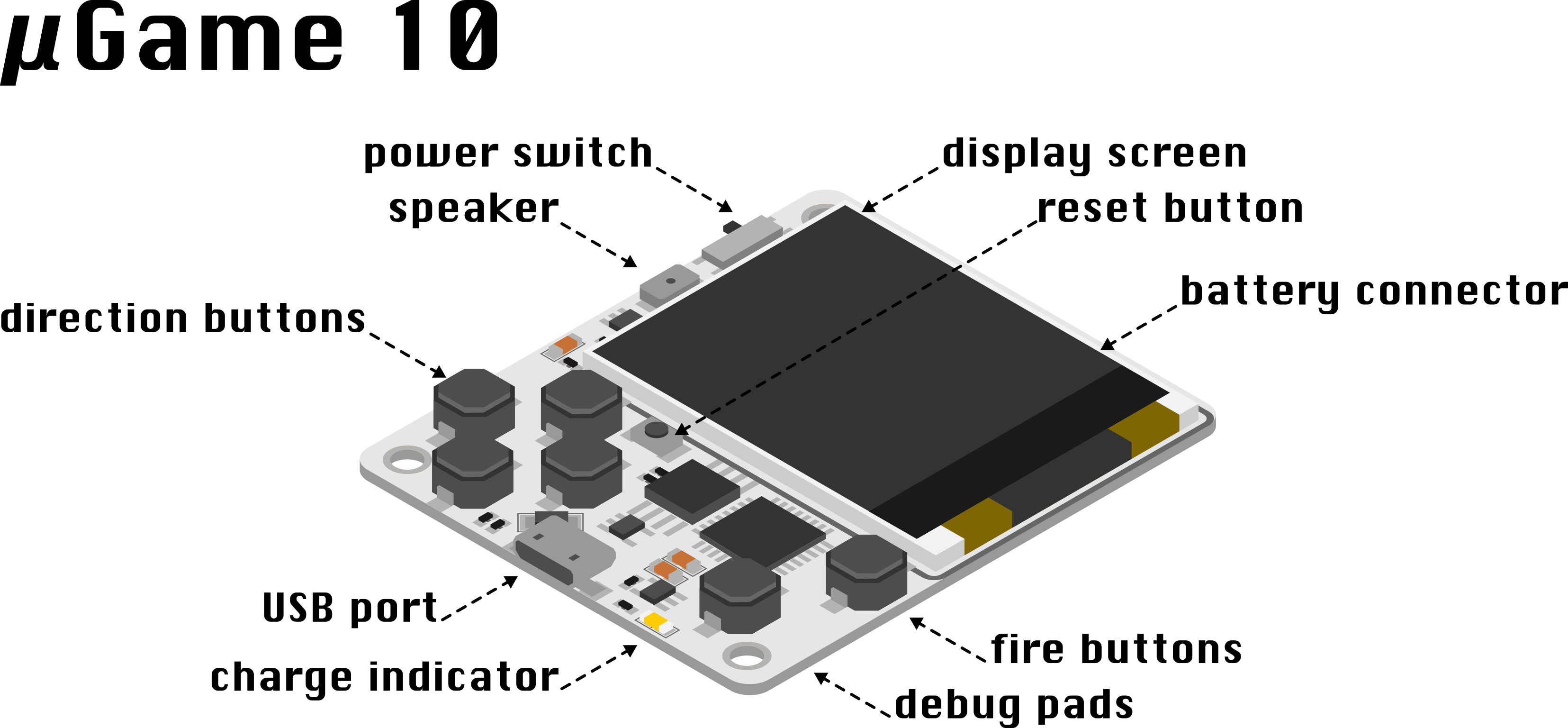
I'm also working on the guide itself, and one of the things I will need is a drawing of the board with the pads marked. So I made this:
I still need to write the actual test program, and see if I can somehow put the CircuitPython and the bootloader into a single binary to be flashed — that would simplify and speed up the process. Unfortunately the test program will still need to be copied over USB — because I also want this and the flash chip tested.
Discussions
Become a Hackaday.io Member
Create an account to leave a comment. Already have an account? Log In.
The testing indeed needed to be in the fab house to avoid the problems when you receive them, especially for further mass production, Very nice project~ waits for your final files.
Are you sure? yes | no