 Jarrett
The @oshpark PCBs have arrived!
Actually they arrived a couple weeks ago, but holiday bustle has kept me away from fun stuff.
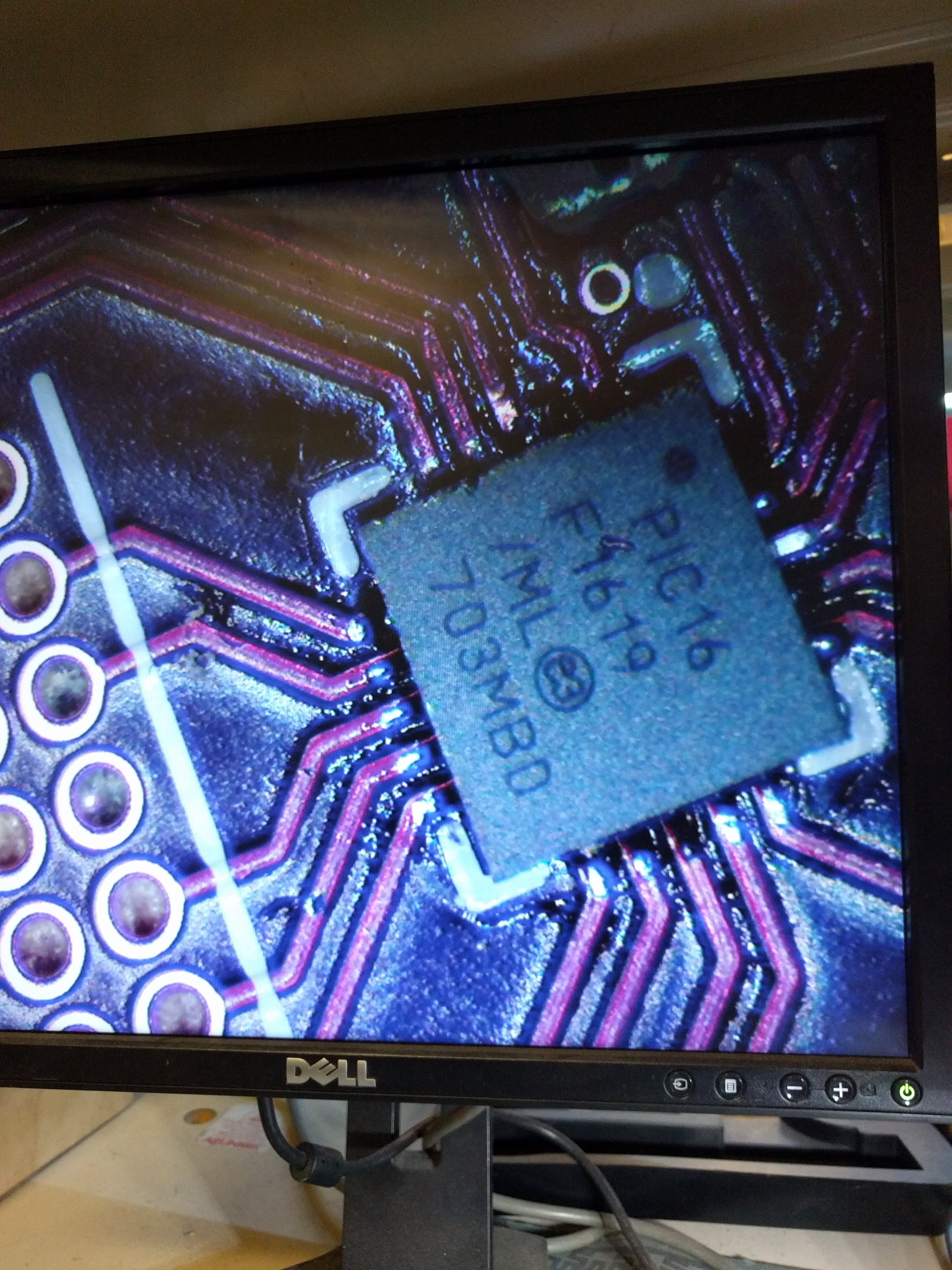
A little bit of reflow, inspection, and touch-up later:
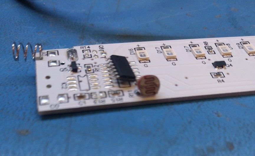
And, to modify the base PCB, a hot air station makes short work of it. Pop up one side of the IC:
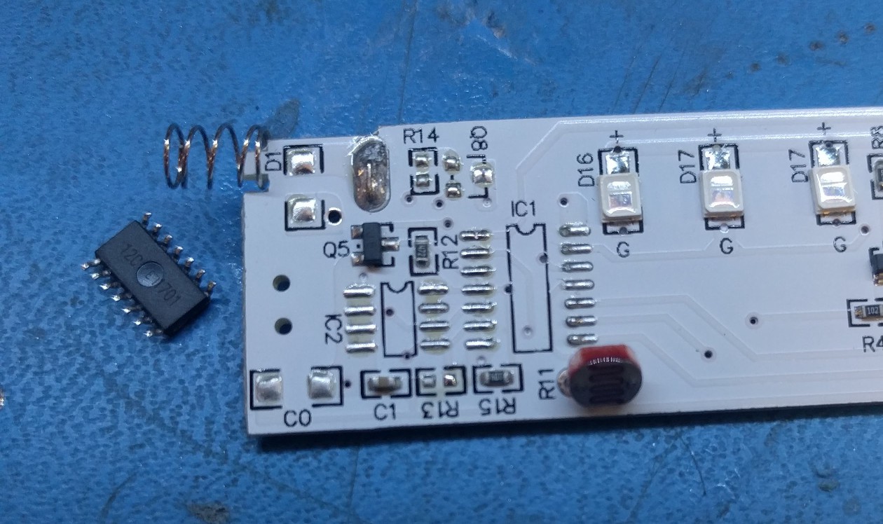
And then the other:
Then the new components are ready to be soldered! 0.65mm isn't that small, good flux, a fine tipped iron and some solder wick are all that's needed to nicely place the headers, flash chip, and the R13 pull-up resistor. I think I used 10k or so.
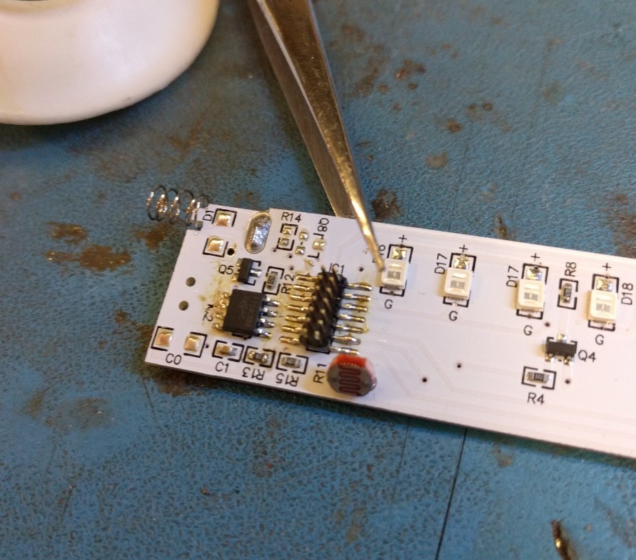
Remember kids: Always clean off your flux before taking the pictures. I didn't do that here, obviously. How embarrassing. This is the reason I don't really like white solder mask.
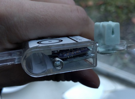
On top of that whole mess goes the daughterboard.
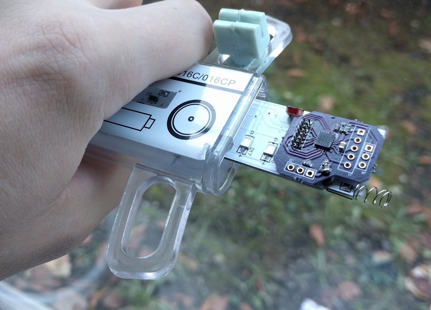
Yeah, that's super low profile.
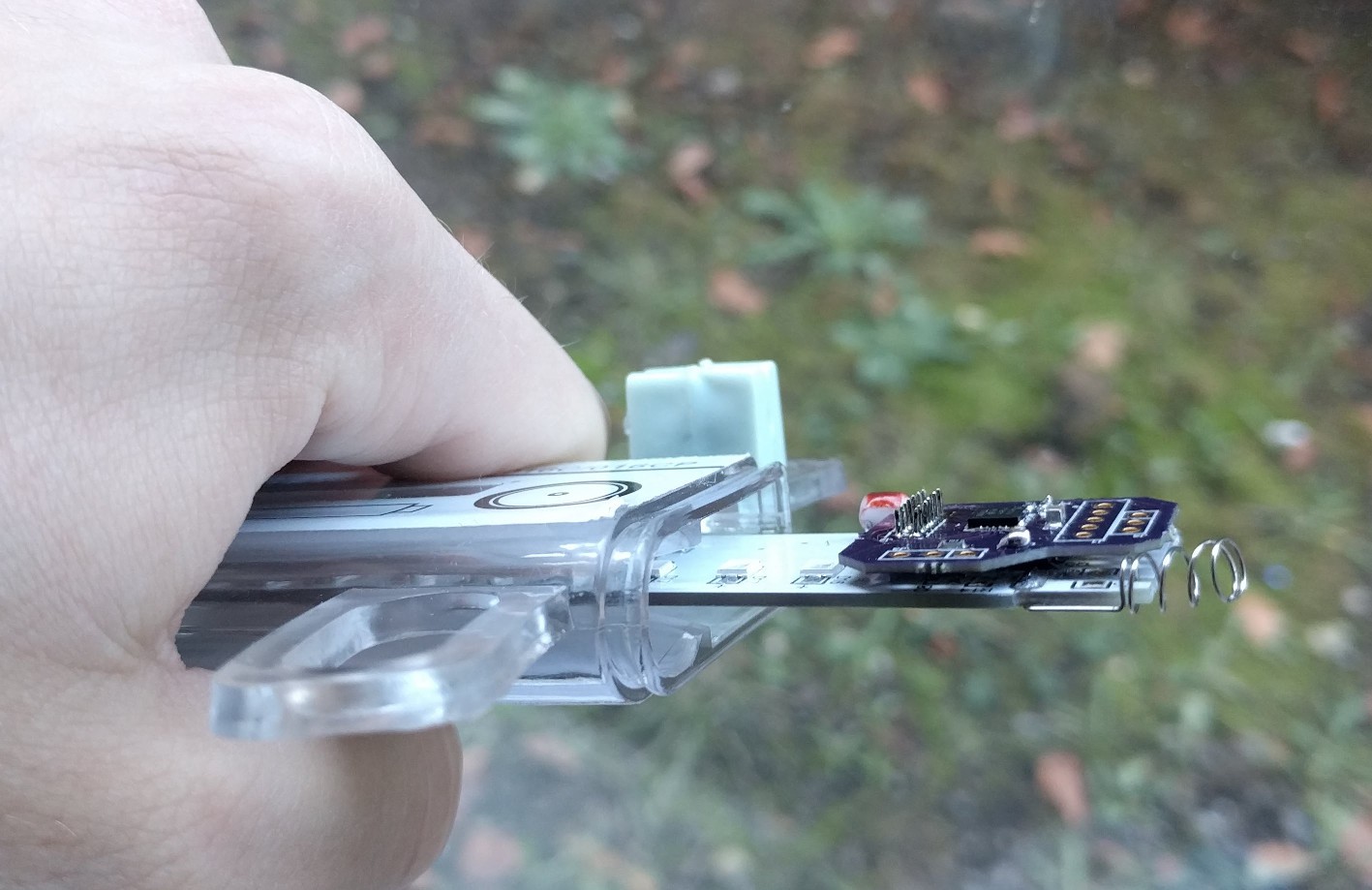
Fits nicely, I like it a lot.
Discussions
Become a Hackaday.io Member
Create an account to leave a comment. Already have an account? Log In.
Very nice!
Are you sure? yes | no