 Christoph
I'll start with this one and write about how I (partially) understand it. It's basically the third schematic from the previous log plus a pull-down resistor for Q2's gate:
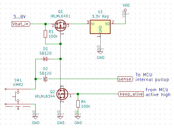
- Vbat_in goes from 3 to 8 V, allowing me to use one or two LiFePO4 cells in series plus some headroom.
- Q1 is a P-channel MOSFET IRLML6401. The allowed V_GS is 8 V so this part is at its maximum rating. I have it in my parts bin mainly for its low gate threshold voltage, a feature which doesn't come into play here. The gate is pulled high by R1, so it's not conducting if not actively pulled down by Q2 or SW1
- SW1 is used to enable power to the regulator and subsequently the MCU.
- Q2 is an N-channel MOSFET IRLML6344. V_GS,th is 1.1 V (max) so it should work well with low-voltage logic input from the keep alive input. The gate is pulled low so it will not conduct if not pulled high actively.
- D1 and D2 (both SB120) because I had those at hand) make sure that, while Q2 is pulling down Q1's gate, the switch state can still be determined by an MCU connected to the sense output.
As soon as SW1 is pressed and the MCU is supplied with power, the MCU has to pull up Q2's gate to keep power enabled. The application can use the sense signal to get input from the push button. If, for example, the button is pressed for more than 1 second, the MCU can run some cleanup code and let go of the keep alive signal.
So much for the theory as I understand it. If you spot any serious flaws in this (especially component choice, since the basic circuit seems to be one that has been proven to work) please leave a comment.
I might remove R4. If this is built as a breadboardable pcb, the user can then choose to either pull Q2's base up or down depending on the application's needs.
Discussions
Become a Hackaday.io Member
Create an account to leave a comment. Already have an account? Log In.
To add flexibility I could break out Q1's gate to a pin header so that beefier transistors can be used instead of the SOT-23 part. As it is now, the circuit needs five pins:
- Gnd
- Vbat_in
- Vbat_out
- sense
- keep_alive
Adding one wouldn't hurt if the pcb is designed to have 2x3 pins. One of the rows could then be G-D-S for the P-channel MOSFET, making it compatible with standard 2,54 mm pitch parts (TO-220)
Are you sure? yes | no
- Need some input and output caps on the regulator
- Imagine that pushbutton gets pressed really sloppily, and it sparks/bounces wildly for 200ms. What happens when the transistors slam on and off uncontrollably? Is there any way to smooth that out?
- How long does it take for a button press to: Make D1 start conducting->Turn on Q1-> Charge up (not yet existent) input cap -> Turn on/stabilise U1-> charge up circuit caps->power up MCU -> read button press. What happens if it takes too long. Is there any way to latch that value?
Are you sure? yes | no
- Reg caps: the regulator is a placeholder and will most probably need an input cap. output shouldn't be relevant to this circuit (or to the part I'm interested in).
- Bouncing button: while the button is closed, current can flow through D1 and charge Q1's gate. It might then be partially on and R1 will turn it off again. As the button bounces a bit more this process is repeated until sometime later the button stops bouncing and/or the MCU circuit pulls Q2's gate high. A pullup on Q2's gate might help here. Or add a cap parallel to the button and a pullup to Vbat_in. Not sure about side effects, though.
- Latching can be done by pulling Q2's gate to Vbat_out instead of pulling it down. Is it necessary to speed up this process? If the MCU doesn't want to keep itself alive it shall choose to die. That problem is imo more on the software side.
Are you sure? yes | no
Regarding bounce: maybe a cap between Q1's gate and Vbat_in (parallel to R1) would help. Pressing the button would quickly charge the cap and keep the transistor on for a longer time.
Are you sure? yes | no