 Paul Andrews
Oh boy, where do you start with LTSpice? That’s precisely the problem I had. It seems like it is purpose built to model power supplies. Perhaps this is a biased point of view though, because that is where I discovered it. However it took me a long time to become comfortable using it - I found it’s interface to be particularly clunky. I’m pretty used to it now though. The one thing I still dislike strongly is how to add new components and sub-circuits to it. And we will need to do that to model my power supply. There is a tutorial here, a dedicated wiki here, and a yahoo group here.
I spent months, literally, simulating my circuit in LTSpice, trying to become comfortable with what each component was doing in the circuit. This is not to say it was difficult, in fact my very first circuits pretty much worked from the start, but past experience had shown me that something that works fine in LTSpice can fail miserably in real life. So I wanted to get comfortable that I had produced the best simulation I could, i.e.:
- Used real-world components rather than ideal components.
- Explored the limits of what the circuit could do in terms of power sources, loads and component variations.
The circuit I ended up using was pretty much lifted straight from the LM3478 datasheet but with a flyback transformer in place of the inductor. TI provide a ton of information about this IC, including how to use it in a flyback converter! You will find a ton of math in these papers. Especially, when it comes to flyback converters, just about every reference you will find is aimed at figuring out what the specification of the transformer should be. This is great if you are going to wind your own transformer. We aren't, we actually want to start with the transformer and work back. I went down the rat hole with these calculations. What I found, in the end, was that most of them don't really matter. The circuit pretty much works out of the box. LTSpice allows you to get close to the right values for the components. A few prototypes let you fine tune it.
What is important is paying attention to the physical characteristics of the board. This was emphasized by Nick de Smith's design for a MAX1771 based Nixie power supply, and rammed home by looking at the datasheet for the LM3478 evaluation board (like I said, TI provide a ton of information about this IC).
Anyway, I digress.
The first thing I did was to download the spice models for the LM3478 and the Wurth Flex Transformers and set them up for LTSpice. Then just forged ahead and entered the circuit. It looks like this:
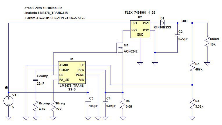
- U1 is the LM3478.
- U2 is the transformer.
- D1 is the output diode. I wasn't picky, I just chose one from the LTSpice standard parts that has a breakdown voltage of around 350V.
- R2 and R3 together set the output voltage. The LM3478 tries to keep the FB pin at 1.26 volts (typically). So the output here should be:
Or 186V (typically).
- Rload would be nixies in a clock. Using 10K here means we are draining 18.6mA. That would be 3mA each for a clock with six tubes.
- V1 is the input voltage, which I have set to 5V.
- Rfreq sets the frequency of the PWM signal being placed on the gate of the MOSFET.
- That MOSFET (AON6242) was just selected from the standard set of MOSFETs that LTSpice knows about. It has a 60V Vds - i.e. it can withstand 60V across the drain-source. 60V should be OK, because we are keeping the output voltage below 200V. So as a rough first estimate, we would expect the maximum voltage on that side of the transformer to be at most 40V. This is because the turns ratio of the transformer is 1:5. So 200/5 is 40.
- Ccomp and Rcomp control the loop compensation - I will get into that later. These values will do for now.
- R4 is the current sense resistor: The LM3478 monitors this and will cut off the MOSFET if the current goes to high. We want the current to stay below the saturation current of the transformer. 0.05 Ohms will do for now.
- The pieces of text that start with a period are LTSpice directives. The first sets up some simulation parameters. The second includes the LM3478 library. The third configures the transformer model.
So how does it do? Here is the output voltage graph:
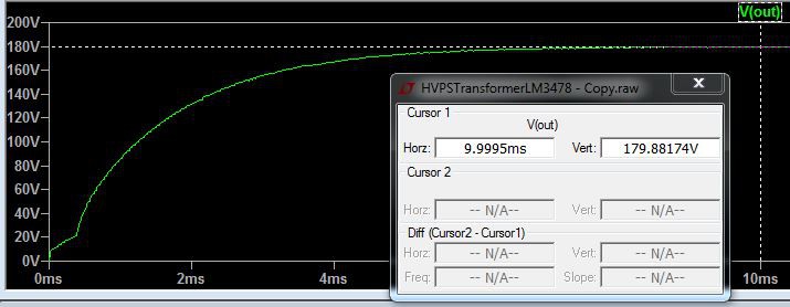
So it gets up to around 180V, which is within the margin of error for the FB voltage monitor (remember 1.26V was typical).
Let's have a look at the Gate of the MOSFET:
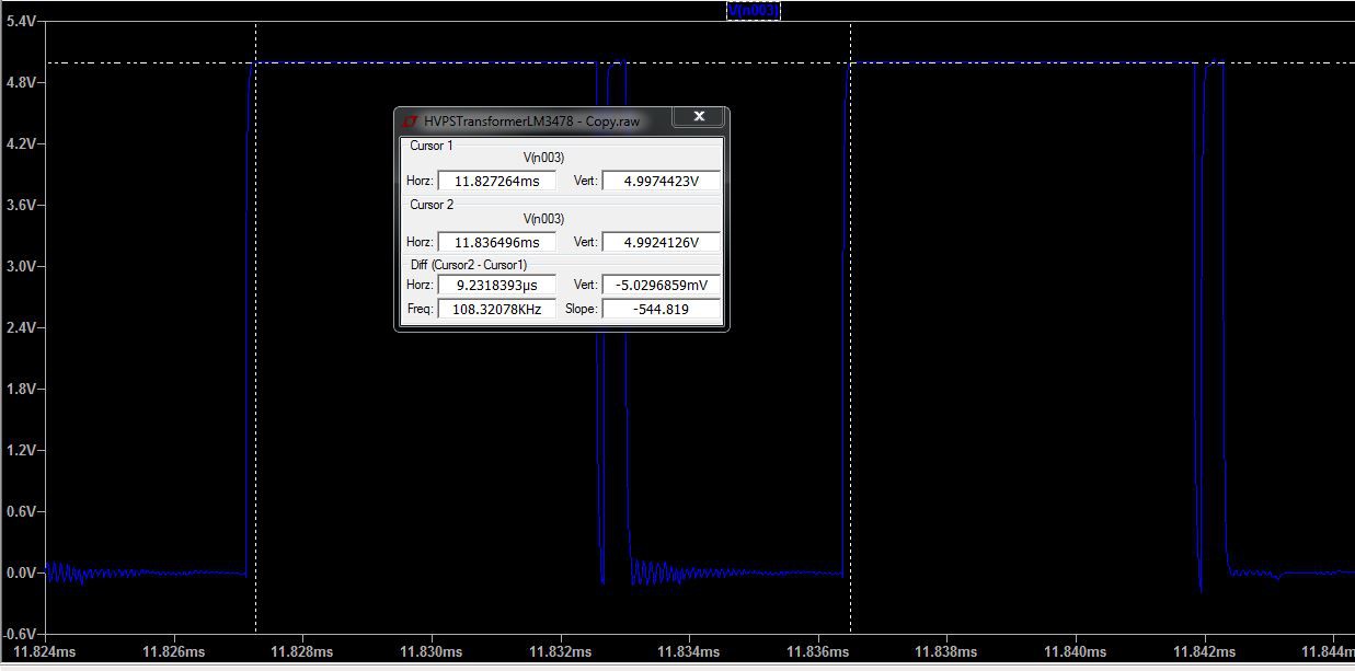
You can see that it is using about a 66% duty cycle at a frequency of around 108KHz.
Now let's look at the Vds (the voltage presented to the drain of the MOSFET):
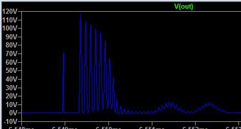
OK. That doesn't look so good. We've got a nice square wave at the gate and an unholy mess on the drain. Look at the peak voltage. 120V. Way beyond the 60V our MOSFET is rated for. This is an example of ringing. It is caused by what are called parasitic inductances and capacitances in the circuit. In this case it is caused by capacitance in the MOSFET and leakage inductance in the transformer.
I will get into all of this later, but right off the bat, we seem to have a circuit that basically works. All we need to do is adjust the components a little. Right? Right?
Discussions
Become a Hackaday.io Member
Create an account to leave a comment. Already have an account? Log In.