The revision 3 PCBs are looking good so far. Since there are components on both sides, I soldered one side with the reflow skillet and the other side by hand.
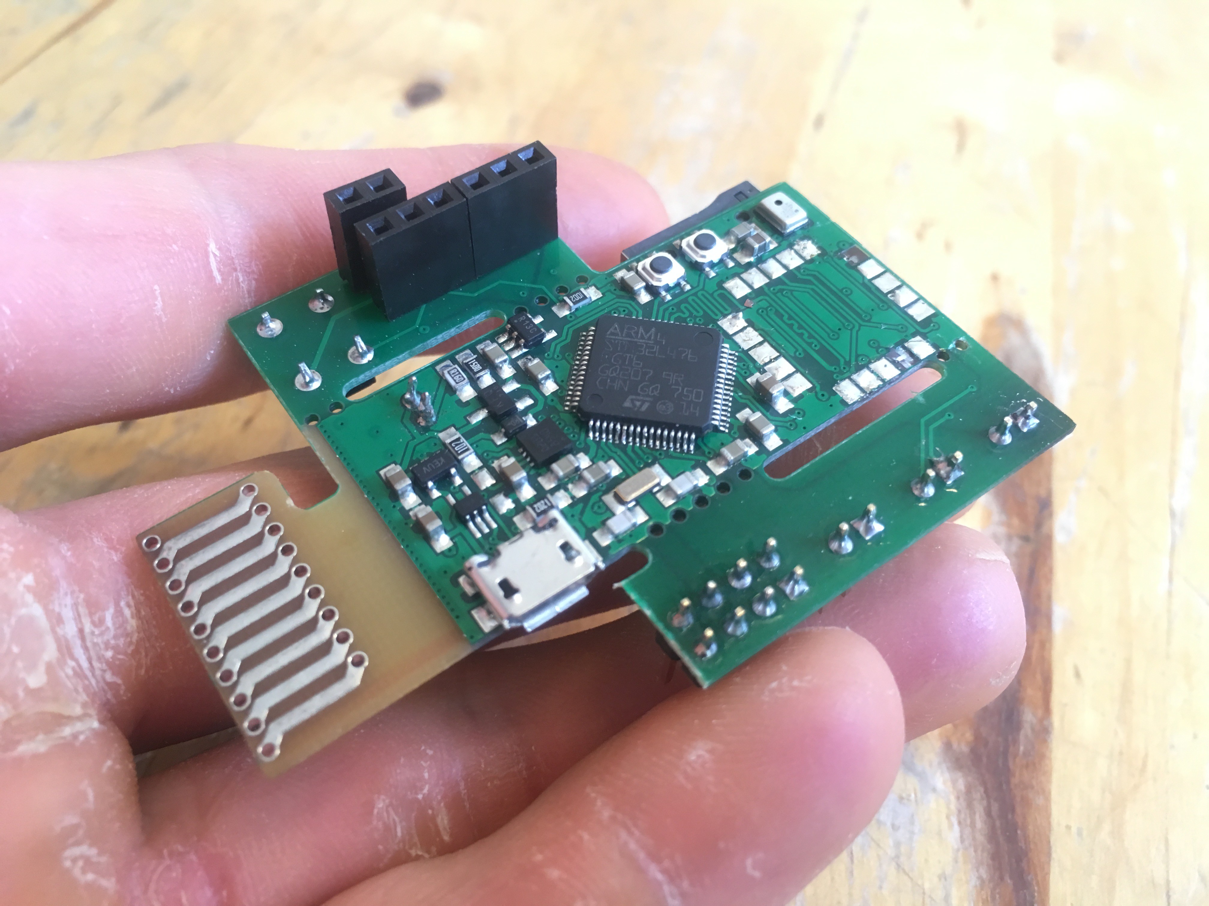
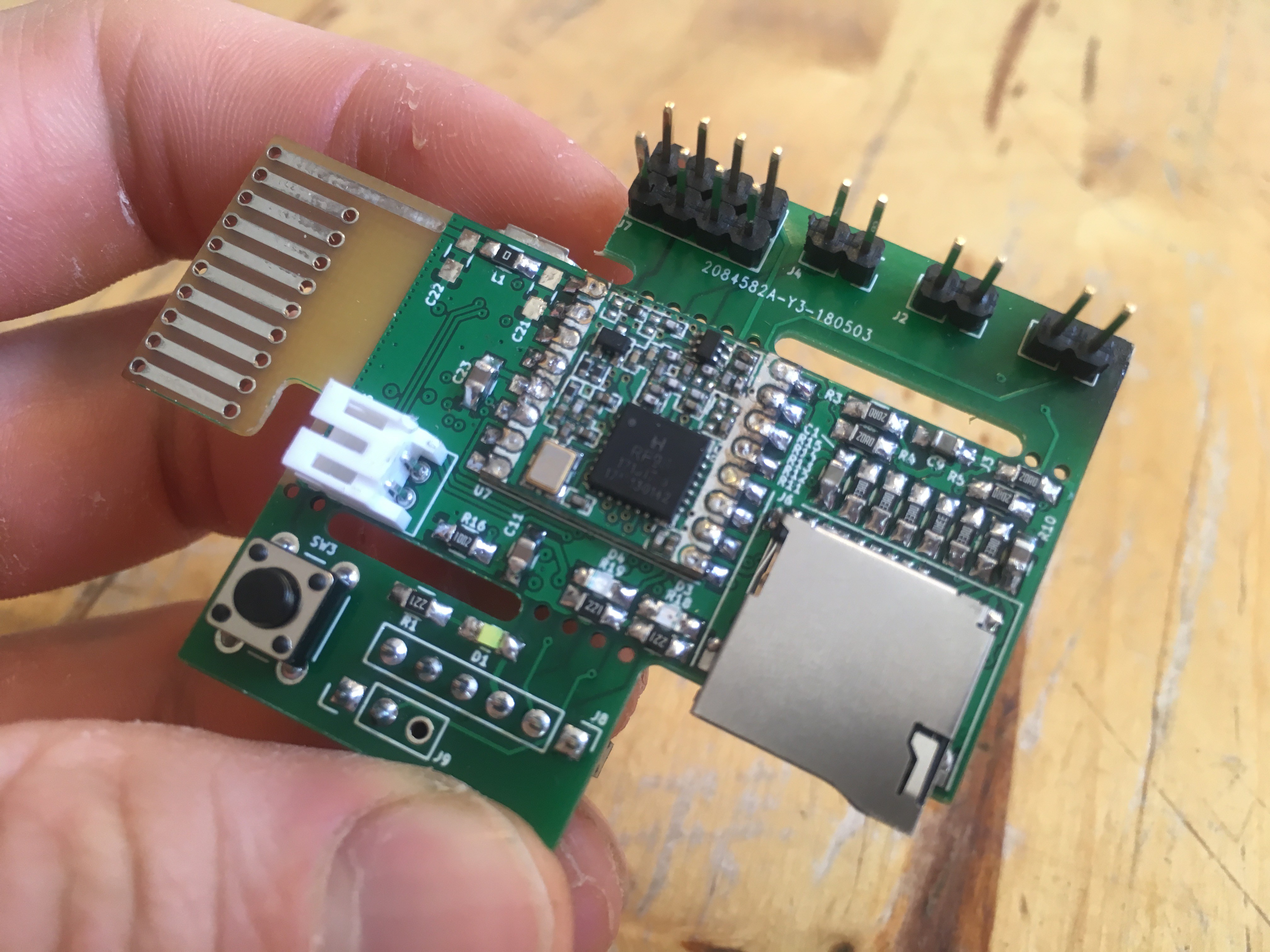
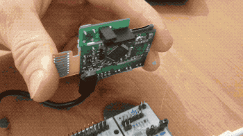
As shown, there are breakaway tabs for a programming header on one side and some broken out signals for debugging on the other. I made the programming header mate with the Nucleo that I've been using as a programmer. It fits nicely:
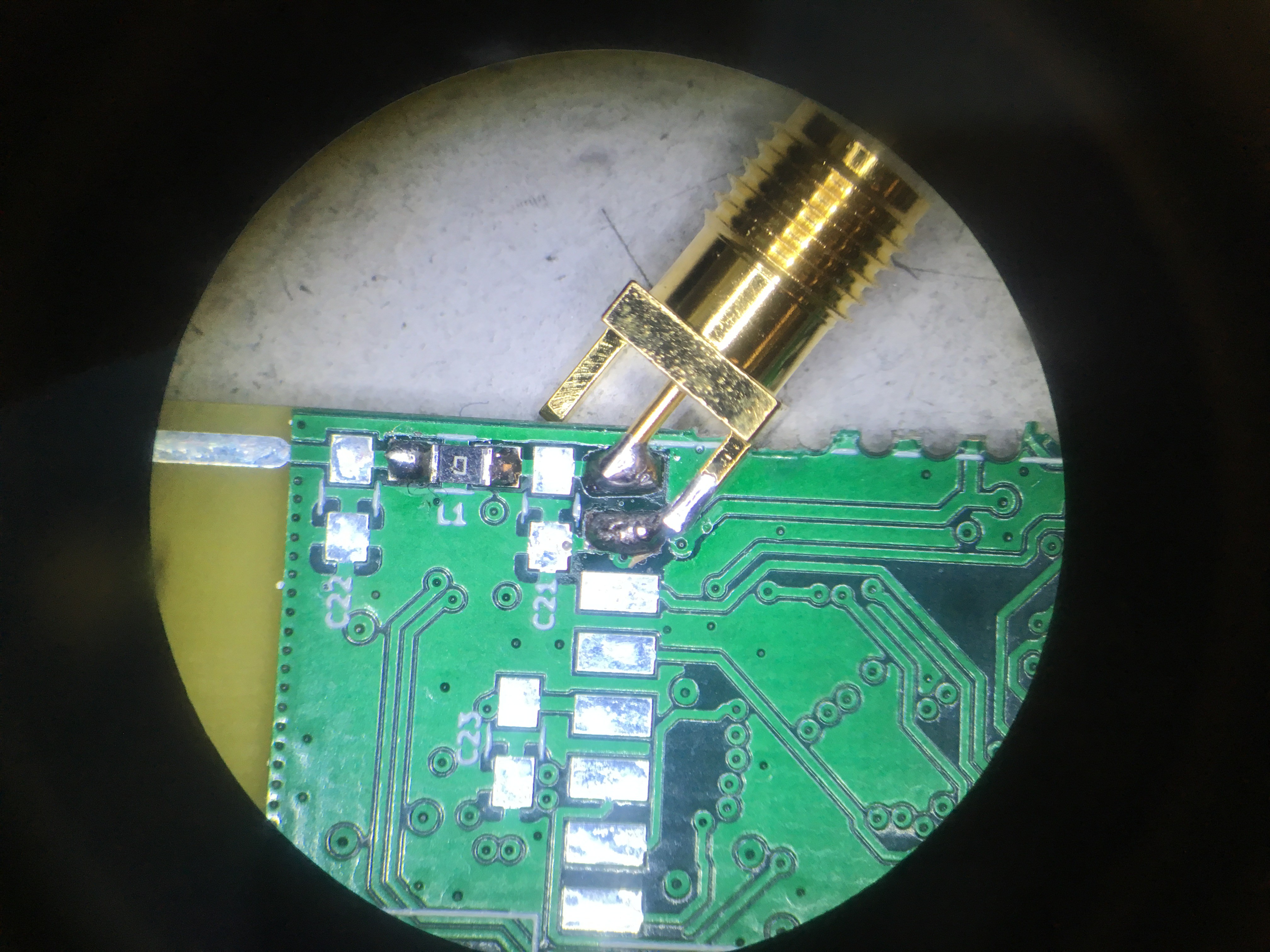
Back to the PCB antenna. In my last post, I explained how I modified it from a TI app note, and simulated to show resonance at 915 MHz. Unfortunately, I also simulated that the impedance would not be very close to 50 ohms, requiring a matching network. This doesn't seem to be the case though. To measure S11 I soldered an SMA connector at the transceivers's ANT pin, and put a 0 ohm resistor where there is a place for a series matching inductor (L1):
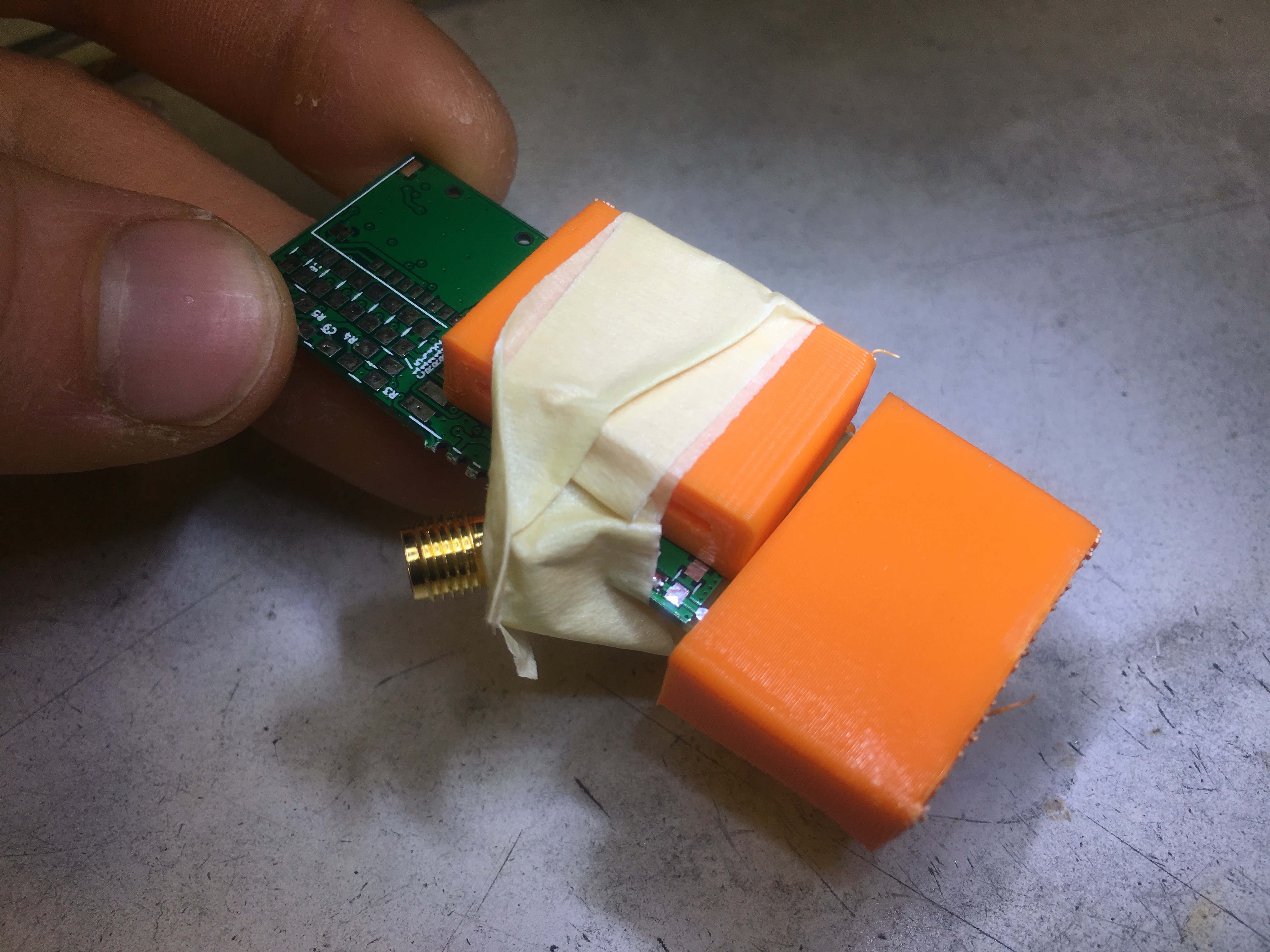
I 3D-printed some ABS covers to put around the antenna to add the effect an enclosure. This plastic shifts the resonance and so I printed a few different thicknesses of cover.

Adding thicker covers shifted the resonance lower, which is what I expected. I decided also to add some ABS material around the rest of the PCB as shown:
With this configuration, I found that the antenna was close to 50 ohms! I thought it was too good to be true, but this is the case. Maybe the parasitics from the unpopulated matching network worked out just perfectly to tune to 50 ohms.
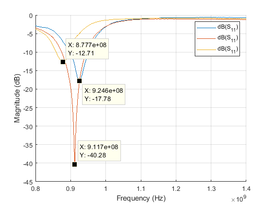
The three traces have an impedances of 49.8 - j58.0 ohm, 52.4 - j1.9 ohm, and 49.3 + j17.6 ohm. Pretty much 50 ohms! No matching network required. :)
Discussions
Become a Hackaday.io Member
Create an account to leave a comment. Already have an account? Log In.