Returning to the problem of replacing manufacturer's boot software with my own, there are several obvious options:
1. remove the boot flash and replace with sockets. Populate the sockets with my own boot flash
2. Pomona makes PLCC probe that clip over the flash. They are pretty expensive and bulky. Maybe too bulky to fit two of them side-by-side on the pc board.
3. Make my own PLCC probe using PLCC sockets.
I don't want to do option 1--too much desoldering and soldering for the number of boards I have. For cost consideration I'll try option 3 first before option 2. I already have a board with boot flash removed and sockets installed so I'll use it to develop my 'hijack' boot software. The purpose of this 'hijack' boot is to take over the board at power up and have a file load utility that load a program into RAM and execute. The program executing in RAM then erases the original flash and reprograms it with my own boot software.
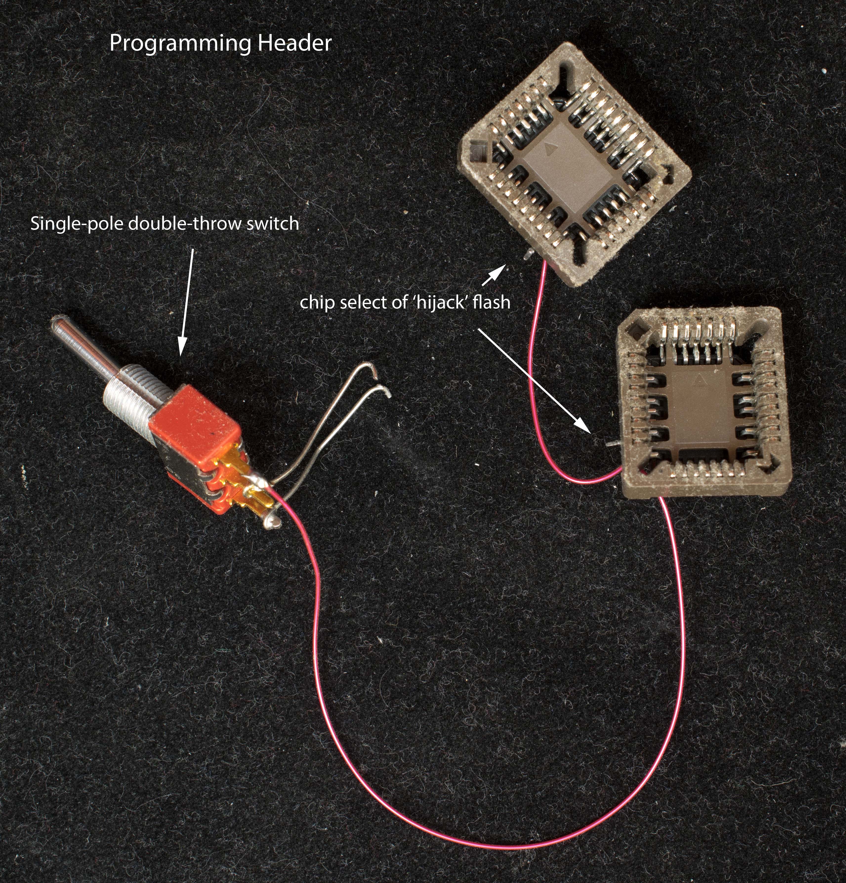
What decides the expensive option 2 vs cheap option 3 is whether a PLCC socket can make reliable contacts with all pins of the original boot flash. The contacts need not last very long, just long enough to load a program into RAM. By process of trials & errors, I found the contacts are actually quite reliable, good for months IF I make sure no solder flux are present on the contacts. So this is my programming header: two 'hijack' flash soldered to PLCC sockets plus a single-pole double-throw (SPDT) switch.

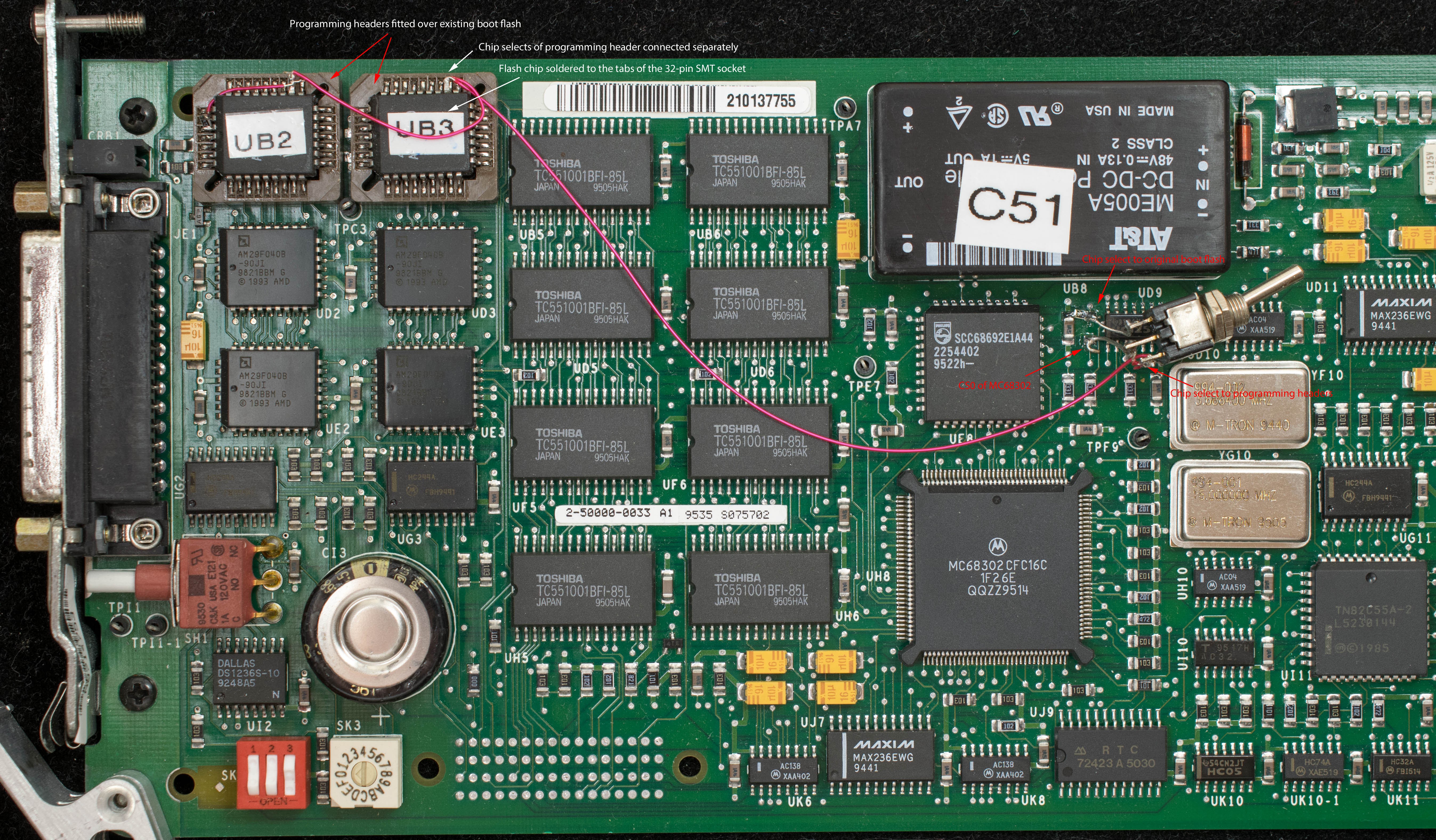
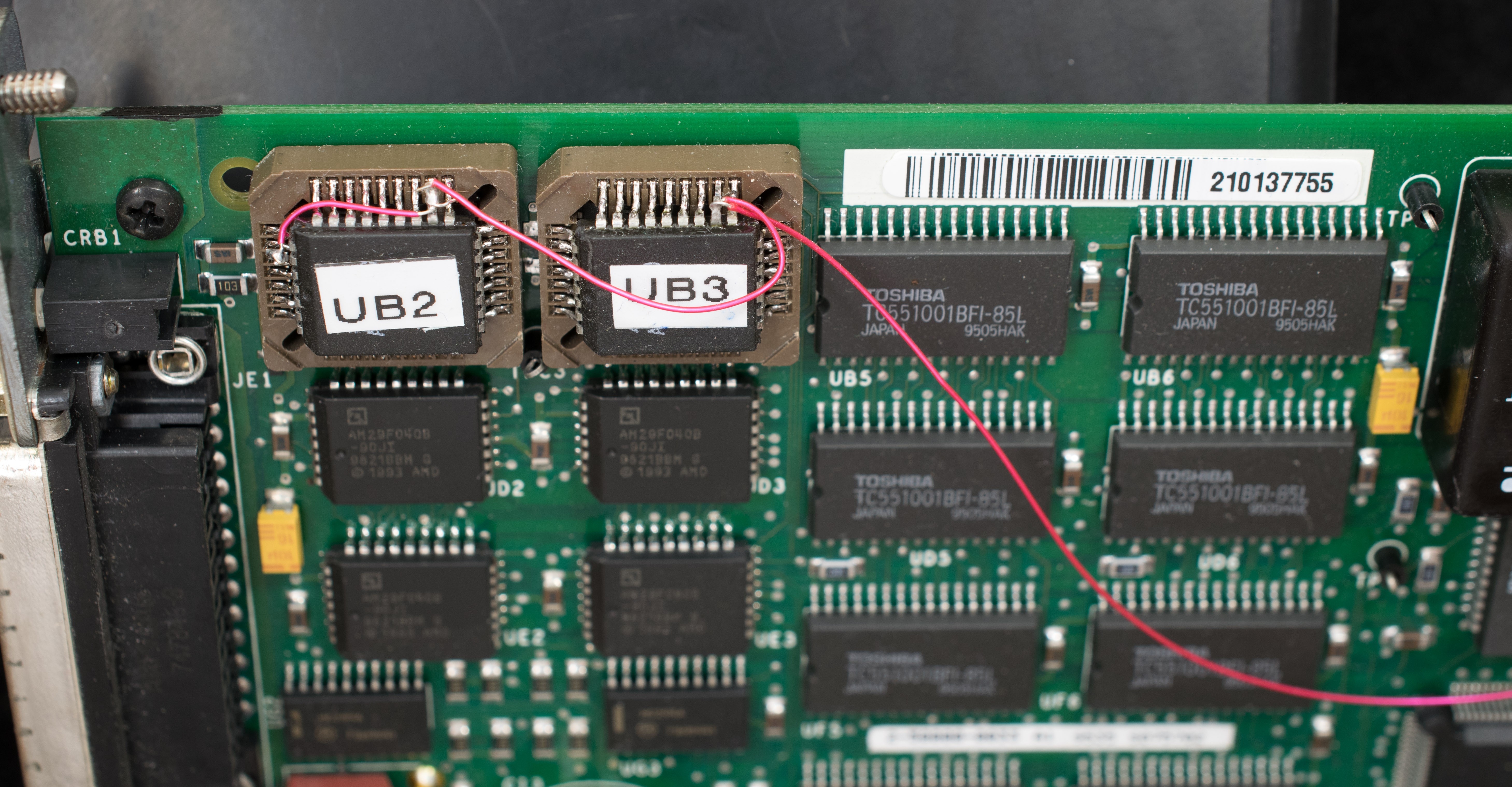
To build the programming header, I first develop a working set of 'hijack' flash using the board that has boot flash in sockets. The 'hijack' flash need to have different device code than the original boot flash (I'll explain why shortly). Once I have a working set of 'hijack' flash, I solder them to the solder tabs of PLCC socket, taking care no flux is on the contacts of the socket. The chip select pins of the 'hijack' flash are bent out and pulled up with a 5K resistor, so the original boot flash's chip selects are separated from the chip selects of the 'hijack' flash. The SPDT switch selects either the chip selects of original boot flash or the chip selects of the 'hijack' flash.


To install the programming header, I fit the PLCC socket over the corresponding original boot flash, press down firmly to make sure it makes good contact. I remove the 330 ohm resistor between chip select 0 of 68302 and chip select of the original boot flash, solder a 5K pull up resistor to the chip select of the original boot flash and solder the remaining two terminal of the switch across the pads of the 330 ohm resistor (the common terminal to the pad leading to 68302 CS0). With the switch set to the programming header, power up. If the installation is done correctly, the 'hijack' flash will sign on and ready to load a program into RAM. This program in RAM will first examine the device code of the flash. If it is not the original boot flash, it will wait until the SPDT is switch over to the original boot flash. Once it recognizes the device code of the original flash, it will erase the flash and copy a new boot software into the original flash. The hijacking is complete, I am now in control of the board!
 Plasmode
Discussions
Become a Hackaday.io Member
Create an account to leave a comment. Already have an account? Log In.