Bharbour
This is a simple little board. It has all of the parts on it to exercise the features of the MCU like the external crystals and USB connector and all of the I/O pins are available on header pins. The crystal pins are shared with the I/O and somewhat sensitive to external capacitance, so there are 3 position jumpers to allow routing them to the crystals or the header pins. Similarly with the USB connector. Jumpers are solder down 0 Ohm resistors to minimize board space and parasitic capacitance.
The SWI/JTAG debug connector used is a 0.050" spaced header that is much smaller than the 0.100" connector that I have been using for ARM projects in the past. Seeing it on this board makes me wish that I had done this years ago. Oh well...
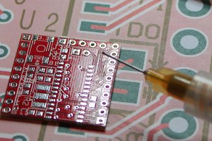
OSH Park did the board fabrication (4 layer) and the first one has been populated. Initial testing looks good, all the oscillators work at the expected frequencies and the debugger hooks up and works.
If anybody is interested in using this board, I can make the files available at OSH Park.
Getting somewhat familiar with this parts basic system stuff like clock generation reminds me why people tend to stick with parts that they are familiar with. I have been through this process a number of times, and it still takes a real chunk of time to do for each device family.

 Analog Two
 Tina Belmont