 Dmitry V. Sokolov
My Christmas decoration:
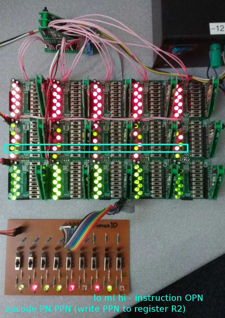
This how the program memory looks like. Those are single pole triple throw slide switches. For the sake of visibility the position of the switches is highlighted with bi-color LEDs. Red light = -1, no light = 0, green light = 1.
The opcodes have 5 trits, so I have 27 5-trit instructions per memory segment. One memory segment is composed of 5 copies of this circuit:
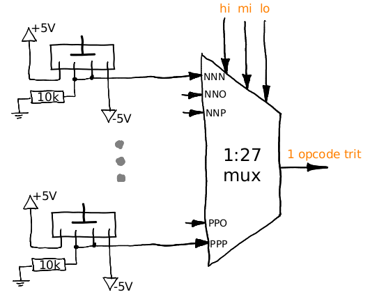
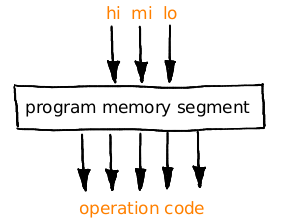
Given a 3-trit address (hi,mi,lo), the 1:27 multiplexor (made with 5 1:3 multiplexers) provides one trit of the corresponding opcode. Thus one memory segment can be seen as a black box that receives a 3-trit address and provides a 5-trit opcode.
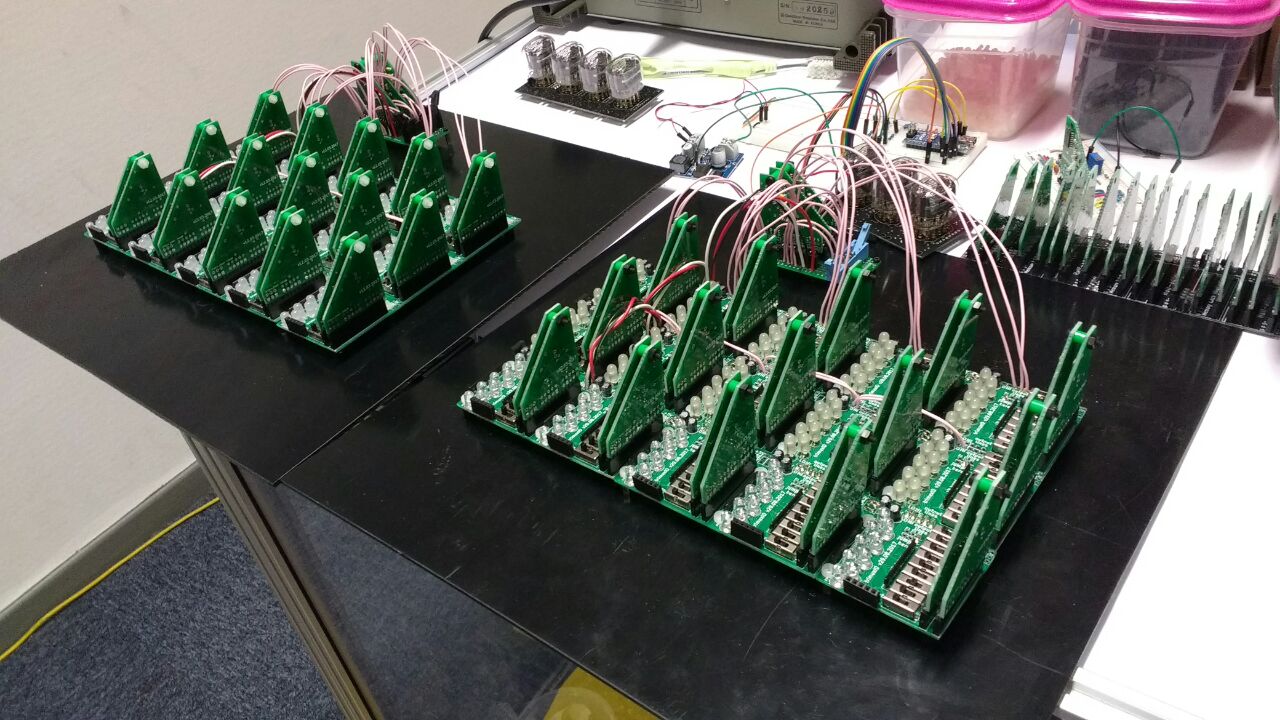
Here I have soldered 2 program memory segments, 54 instructions total. The architecture supports up to 27 memory segments (27*27=729 instructions).
Discussions
Become a Hackaday.io Member
Create an account to leave a comment. Already have an account? Log In.