 Dmitry V. Sokolov
-
Ternary computer program emulator
04/04/2020 at 13:06 • 0 commentsTo ease the debugging phase, here is an emulator for the ternary programs:
https://github.com/ssloy/triador
A very simple sample program that computes R2+R3 and stores the results back in R3:
R1 NNN # N.B. the memory is not guaranteed to be initialized RR NNN # initialize R13 with -13, this chooses segment NNN for jumps R2 ONP # write -2 to R2 ┌─────────────────────────────────┐ R3 PPP # write 13 to R3 │ This program computes R2+R3, │ RR OPO # copy R3 to R1 <─┐ │ the result is stored in R3. │ SK NPO # skip if R2!=0 │ │ Here is a C++ world equavalent: │ JP PNO # R2==0, terminate│ ────┐ │ │ SK PNP # skip if R2>0 │ │ │ int R2 = -2; │ RR OON # R1-- │ │ │ int R3 = 13; │ SK PNN # skip if R2<0 │ │ │ while (R2!=0) { │ RR OOP # R1++ │ │ │ int R1 = R3; │ RR ONO # copy R1 to R3 │ │ │ if (R2>0) R1++; │ RR OPN # copy R2 to R1 │ │ │ if (R2<0) R1--; │ SK PNP # skip if R2>0 │ │ │ R3 = R1; │ RR OOP # R1++ │ │ │ R1 = R2; │ SK PNN # skip if R2<0 │ │ │ if (R2>0) R1--; │ RR OON # R1-- │ │ │ if (R2<0) R1++; │ RR ONP # copy R1 to R2 │ │ │ R2 = R1; │ JP NOO # jump here ──────┘ │ │ } │ EX PPP # halt and catch fire <─┘ └─────────────────────────────────┘ -
Homebrew ternary mini-series (s1e5): random-access memory board
04/04/2020 at 13:04 • 0 commentsCheck for the subtitles if you do not speak russian.
-
Homebrew ternary mini-series (s1e4): memory cell
04/04/2020 at 13:03 • 0 comments -
Homebrew ternary mini-series (s1e3): multiplexers
04/04/2020 at 13:02 • 0 commentsCheck for the subtitles if you do not speak russian.
-
Homebrew ternary mini-series (s1e2): balanced ternary basics
03/31/2020 at 09:10 • 0 commentsCheck for the subtitles if you do not speak russian.
-
Homebrew ternary mini-series (s1e1): IO card
03/31/2020 at 09:09 • 0 commentsCheck for the subtitles if you do not speak russian.
-
TRIADOR ALU
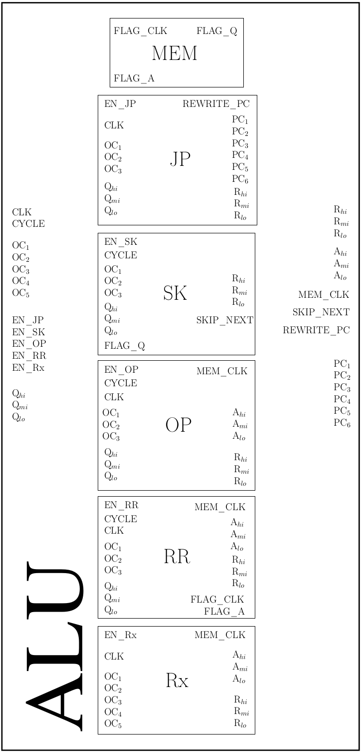
07/10/2018 at 19:39 • 0 commentsBack to the true ternary triador implementation. The ALU will look like this:
![]()
Compare it to the overall schematics of the triador in the project details. All input signals are shown on the left of the boxes, all output signals are on the right. The ALU consists of 5 slices (one per operation) plus one trit memory cell for the borrow/carry flag. This flag won't be accessible outside of the ALU, its value is set by the RR slice, and is read by the SK slice only.
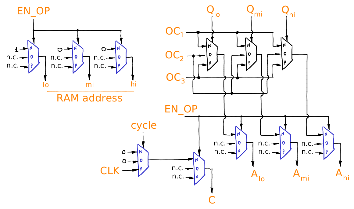
Just to give you an idea of what the boxes look inside, here is the OP box (tritwise unary operation over R1 register):
![]()
-
Ternary counter on VHDL
07/08/2018 at 09:26 • 2 commentsI just literally copied this ternary counter design from 2011 into VHDL:
![]()
This is VHDL source code (only 3 trits were used):
library IEEE;
use IEEE.STD_LOGIC_1164.ALL;

use ternary.all;

entity main is
    Port ( clk : in bit;
           res : in bit;
           a : in FakeTrit;
           b : in FakeTrit;
           c : in FakeTrit;
           s1 : out FakeTrit;
           s2 : out FakeTrit;
           s3 : out FakeTrit;
           led : out bit);
end main;

architecture Behavioral of main is
signal a1,b1,c1,ss0,ss1,ss2,ss3,ss4 : FakeTrit;
signal pclk,pclk1,nclk,nclk1,res0,res1,m1,m2,m3,m4,h1,h2,h3,h4,g1,g2,g3 : FakeTrit;
signal tmp_clk_std, tmp_iclk_std : STD_LOGIC;
signal tmp_clk : BIT;

COMPONENT Clock_Divider
PORT(
clk : IN std_logic;
reset : IN std_logic;
clock_out : OUT std_logic
);
END COMPONENT;

COMPONENT Half_Adder
Port ( a : in FakeTrit;
       b : in FakeTrit;
       s : out FakeTrit;
       c : out FakeTrit
      );
END COMPONENT;

FUNCTION io_invert(T: FakeTrit) RETURN FakeTrit IS
begin
                case T is
                when N =>
                        return P;
                when O =>
                        return X;
                when P =>
                        return N;
                when others =>
                        return O;
                end case;
end;

begin

a1 <= io_invert(a);
b1 <= io_invert(b);
c1 <= io_invert(c);

tmp_iclk_std <= to_stdulogic(clk);
div1: Clock_Divider port map( clk => tmp_iclk_std, reset => '0', clock_out => tmp_clk_std );
tmp_clk <= to_bit(tmp_clk_std);

res0(0) <= '0';
res0(1) <= res;
res1 <= res0;

clk1: ternary_clock port map( B_C => tmp_clk, T_C => ss0 );
mux1: ternary_mux port map( T_S => ss0, T_N => O, T_O => O, T_P => P, T_C => pclk );
mux2: ternary_mux port map( T_S => res1, T_N => pclk, T_O => N, T_P => N, T_C => pclk1 );
mux3: ternary_mux port map( T_S => ss0, T_N => N, T_O => O, T_P => O, T_C => nclk );
mux4: ternary_mux port map( T_S => res1, T_N => nclk, T_O => P, T_P => P, T_C => nclk1 );

mem1: ternary_mem port map( T_S => pclk1, T_N => O, T_P => ss1, T_Q => m1 );
ha1: Half_Adder port map( a => P, b => m1, s => h1, c => g1 );
mem2: ternary_mem port map( T_S => nclk1, T_N => h1, T_P => O, T_Q => ss1 );

mem3: ternary_mem port map( T_S => pclk1, T_N => O, T_P => ss2, T_Q => m2 );
ha2: Half_Adder port map( a => g1, b => m2, s => h2, c => g2 );
mem4: ternary_mem port map( T_S => nclk1, T_N => h2, T_P => O, T_Q => ss2 );

mem5: ternary_mem port map( T_S => pclk1, T_N => O, T_P => ss3, T_Q => m3 );
ha3: Half_Adder port map( a => g2, b => m3, s => h3, c => g3 );
mem6: ternary_mem port map( T_S => nclk1, T_N => h3, T_P => O, T_Q => ss3 );

s1 <= io_invert(ss1);
s2 <= io_invert(ss2);
s3 <= io_invert(ss3);

led <= to_bit(tmp_clk_std);

end Behavioral;
Every trit in the counter takes 2 macrocells on CoolRunner-II, so technically CoolRunner-II chip XC2C256 with 256 macrocells may have up to 128-trit counter inside! This is pin assignments for XC2-XL board (a,b,c are not used here):
NET "clk" LOC = "P38" | IOSTANDARD = LVTTL ;
NET "res" LOC = "P143" | IOSTANDARD = LVTTL ;
NET "a<0>"  LOC = "P140" | IOSTANDARD = LVTTL ;
NET "a<1>"  LOC = "P142" | IOSTANDARD = LVTTL ;
NET "b<0>"  LOC = "P138" | IOSTANDARD = LVTTL ;
NET "b<1>"  LOC = "P139" | IOSTANDARD = LVTTL ;
NET "c<0>"  LOC = "P136" | IOSTANDARD = LVTTL ;
NET "c<1>"  LOC = "P137" | IOSTANDARD = LVTTL ;
NET "s3<0>"  LOC = "P82" | IOSTANDARD = LVTTL ;
NET "s3<1>"  LOC = "P83" | IOSTANDARD = LVTTL ;
NET "s2<0>"  LOC = "P85" | IOSTANDARD = LVTTL ;
NET "s2<1>"  LOC = "P86" | IOSTANDARD = LVTTL ;
NET "s1<0>"  LOC = "P87" | IOSTANDARD = LVTTL ;
NET "s1<1>"  LOC = "P88" | IOSTANDARD = LVTTL ;
NET "led"  LOC = "P92" | IOSTANDARD = LVTTL ;
and this is a video that proves that it's working on Xilinx CoolRunner-II ;)
-
Ternary VHDL package v1.0 is ready
07/06/2018 at 09:30 • 0 commentsSo now we have everything to build a ternary computer in binary CPLD (or FPGA)::
https://cdn.hackaday.io/files/285791222723936/ternary.vhd
Last pieces were just added:
- procedure dmux:
        PROCEDURE dmux(signal T_S: IN FakeTrit;
                       signal T_C: IN FakeTrit;
                       signal T_N: OUT FakeTrit;
                       signal T_O: OUT FakeTrit;
                       signal T_P: OUT FakeTrit) IS
        begin
                case T_S is
                when N =>
                        T_N <= T_C;
                        T_O <= O;
                        T_P <= O;
                when O =>
                        T_N <= O;
                        T_O <= T_C;
                        T_P <= O;
                when P =>
                        T_N <= O;
                        T_O <= O;
                        T_P <= T_C;
                when others =>
                        T_N <= X;
                        T_O <= X;
                        T_P <= X;
                end case;
        end;
- component ternary_mem:
-- Entity ternary_mem

USE ternary.ALL;

ENTITY ternary_mem IS
        PORT (
              T_S : IN FakeTrit;
              T_N : IN FakeTrit;
              T_P : IN FakeTrit;
              T_Q : OUT FakeTrit
        );
END ternary_mem;

ARCHITECTURE Behavioral OF ternary_mem IS
BEGIN
    PROCESS (T_S)
    BEGIN
        IF (T_S(0) = '1') THEN
            T_Q <= T_P;
        ELSIF (T_S(1) = '1') THEN
            T_Q <= T_N;
        END IF;
    END PROCESS;
END Behavioral;
- component ternary_clock:-- Entity ternary_clock USE ternary.ALL; ENTITY ternary_clock IS PORT ( B_C : IN BIT; T_C : OUT FakeTrit ); END ternary_clock; ARCHITECTURE Behavioral OF ternary_clock IS signal flag : bit; BEGIN PROCESS (B_C) BEGIN IF (B_C'event AND B_C = '1') THEN IF (flag = '0') THEN flag <= '1'; ELSE flag <= '0'; END IF; END IF; IF (B_C = '1' AND flag = '0') THEN T_C(0) <= '1'; ELSE T_C(0) <= '0'; END IF; IF (B_C = '1' AND flag = '1') THEN T_C(1) <= '1'; ELSE T_C(1) <= '0'; END IF; END PROCESS; END Behavioral;Last one turns binary clock into ternary sequence NOPONOPONOPO...
Also I renamed some variable names and added additional components for mux and dmux ( just in case if somebody doesn't like them as functions ; )
-
Interfacing ternary and binary components
07/05/2018 at 04:15 • 0 commentsOk, now it is kind of proven that binary CPLD (or FPGA) may implement ternary logic, but how we can integrate it with "true" ternary components, especially when CPLD is 3.3V and TRIMUXes are -5V and +5V? Answer is DG403 chips may do the job:
![]()
Because simplified ternary mutexes e12 and e21 can be easily implemented by DG403 integrated circuits:
![]() So we need to have ONE DG403 per every binary represented TRIT and it doesn't matter if it's input or output, but number of inputs should be multiple by 2 in order to use DG403 chips optimally.
So we need to have ONE DG403 per every binary represented TRIT and it doesn't matter if it's input or output, but number of inputs should be multiple by 2 in order to use DG403 chips optimally.
Also we can do similar interfacing for binary ROM or RAM that may also be required for complex ternary systems. For example we can do translation from triad (3 trits) to a byte the same way how it's already done in 3niti alpha simu1 ternary computer simulator on PIC16:;Format of the triad: ;|7|6|5|4|3|2|1|0| ;|+|-|+|-|+|-|+|-| ;|par|low|mid|high ;par (parity) is not yet used, so it's always 0 0 for now... tOOO EQU 0x00 ; 0 tNOO EQU 0x01 ; -9 tPOO EQU 0x02 ; +9 tONO EQU 0x04 ; -3 tNNO EQU 0x05 ; -12 tPNO EQU 0x06 ; +6 tOPO EQU 0x08 ; +3 tNPO EQU 0x09 ; -6 tPPO EQU 0x0A ; +12 tOON EQU 0x10 ; -1 tNON EQU 0x11 ; -10 tPON EQU 0x12 ; +8 tONN EQU 0x14 ; -4 tNNN EQU 0x15 ; -13 tPNN EQU 0x16 ; +5 tOPN EQU 0x18 ; +2 tNPN EQU 0x19 ; -7 tPPN EQU 0x1A ; +11 tOOP EQU 0x20 ; +1 tNOP EQU 0x21 ; -8 tPOP EQU 0x22 ; +10 tONP EQU 0x24 ; -2 tNNP EQU 0x25 ; -11 tPNP EQU 0x26 ; +7 tOPP EQU 0x28 ; +4 tNPP EQU 0x29 ; -5 tPPP EQU 0x2A ; +13As you can see we directly translate triad to byte and vice versa for data, but we can do the same for address - lower 3 trit of address can address the same 48 bytes (so instead of 27 triad one page will occupy 48 bytes of binary memory). Higher trits of address may or may not have similar translation.
Also we can have a special CPLD that converts ternary address to binary address optimally (without gaps and holes as above). Below you can see calculations for mostly used memory sizes:
2KB = 11-bit address = 6 trits (729 ternary cells - 28% used);
8KB = 13-bit address = 8 trits (6,561 ternary cells - 63% used);
32KB = 15-bit address = 9 trits (19,683 ternary cells - 48% used);
64KB = 16-bit address = 10 trits (59,049 ternary cells - 71% used);
128KB = 17-bit address = the same 10 trits (59,049 ternary cells - 45% used);
256KB = 18-bit address = 11 trits (177,147 ternary cells - 67% used);
512KB = 19-bit address = the same 11 trits (177,147 ternary cells - almost 34% used);
1MB = 20-bit address = 12 trits (531,441 ternary cells - almost 51% used).
As you can see we have better usage of binary memory in ternary computer system when it's 64KB addressed by 10 trits and this approach will use 71% of memory space.
In case of TRIADOR we have 6-trit address for program memory - it has addresses from -364 to +364 and each read-only memory cell should have 5-trit value - to simplify things in my Logisim model I addressed 2K binary ROM directly when every TRIT of ternary address is converted to 2 BITS of binary address, but in this case it has to be 12 bits total, but we have only 11 (2^11=2048) - my idea was to allow user to use ternary addresses from ONNNNN to PPPPPP only (it is 66% of all 6-trit address space and should be more than enough for start) and we need to convert 1-byte data to 5-trit program word by another smaller ROM (or CPLD):<comp lib="4" loc="(850,300)" name="ROM"> <a name="dataWidth" val="10"/> <a name="contents">addr/data: 8 10 0 1 6 4 5 1a 18 19 12 10 11 16 14 15 6a 68 69 62 60 61 66 64 65 4a 48 49 42 40 41 46 44 45 5a 58 59 52 50 51 56 54 55 1aa 1a8 1a9 1a2 1a0 1a1 1a6 1a4 1a5 18a 188 189 182 180 181 186 184 185 19a 198 199 192 190 191 196 194 195 12a 128 129 122 120 121 126 124 125 10a 108 109 102 100 101 106 104 105 11a 118 119 112 110 111 116 114 115 16a 168 169 162 160 161 166 164 165 14a 148 149 142 140 141 146 144 145 15a 158 159 152 150 151 156 154 155 13*0 2aa 2a8 2a9 2a2 2a0 2a1 2a6 2a4 2a5 28a 288 289 282 280 281 286 284 285 29a 298 299 292 290 291 296 294 295 22a 228 229 222 220 221 226 224 225 20a 208 209 202 200 201 206 204 205 21a 218 219 212 210 211 216 214 215 26a 268 269 262 260 261 266 264 265 24a 248 249 242 240 241 246 244 245 25a 258 259 252 250 251 256 254 255 aa a8 a9 a2 a0 a1 a6 a4 a5 8a 88 89 82 80 81 86 84 85 9a 98 99 92 90 91 96 94 95 2a 28 29 22 20 21 26 24 25 a 8 9 2 </a> </comp>
If you have some ideas to share - feel free to participate in our public chat:
Homebrew ternary computer
TRIADOR: The only ternary computer made for real in the past 50 years.

 So we need to have ONE DG403 per every binary represented TRIT and it doesn't matter if it's input or output, but number of inputs should be multiple by 2 in order to use DG403 chips optimally.