 Ted Yapo
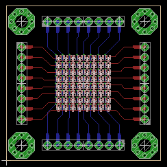
I've done a few projects where I need mating PCBs for some reason - holes or header connectors or both have to fit together. And, I've screwed a few of them up. For example, the top PCB in one sandwich I'm working on looks like this:
To get the mounting holes and headers in the right place, I decided to make a "template" PCB footprint that I could include on each board to make sure the mating components line up.
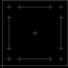
This "component" has registration marks in the "reference" layer for the centers of the mating components, and the board origin, outline, and center. With this, it's easy to make the other PCB(s) fit exactly:
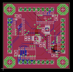
No more messed up PCBs (for this reason, anyway).
Discussions
Become a Hackaday.io Member
Create an account to leave a comment. Already have an account? Log In.