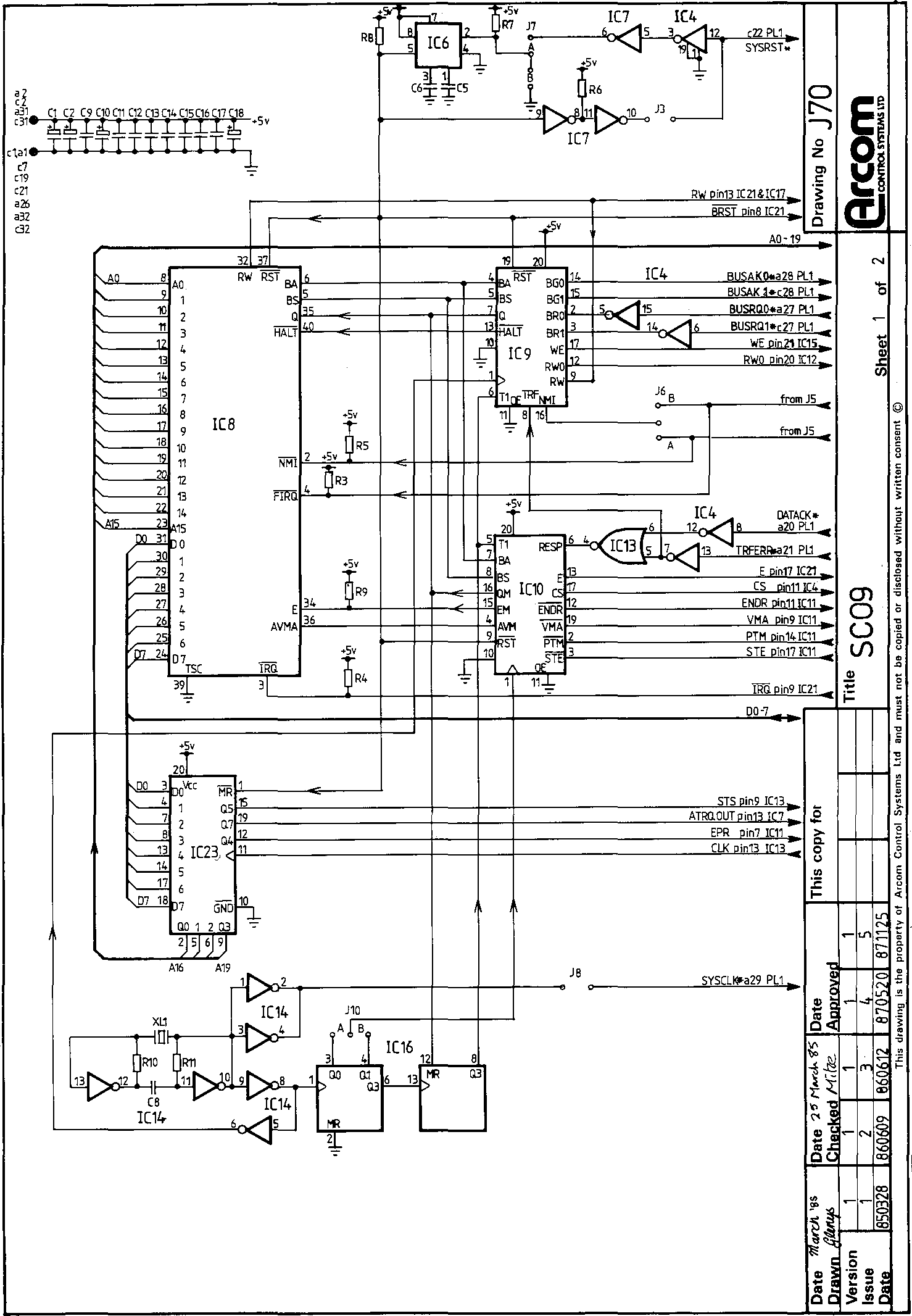
We start by looking at the Arcom SC09 board, see Figure 6.26(a). IC8 is the 680B09E processor and its E and Q clocks are produced by PAL IC10.
However, since the data could take some time arriving when an STEbus access is performed, the E and Q clocks are stopped during the STEbus access, thus ‘halting’ the 6809. IC10 waits for RESP to go LO (DATACK* or TRFERR* asserted) before releasing the processor from its stopped state. The maximum amount of time a 6809 can have its clocks stopped is 10 µs if it is left longer than this it can lose the contents of its internal registers. To prevent this happening IC16, a counter, drives Q3 HI after 8 µs, and when IC10 sees Q3 go HI it restarts the clocks. The timeout signal is also sent to IC9, another PAL, which triggers the 6809’s /NMI line, thus informing the processor that a timeout has occurred. A timeout can occur for two reasons: either a slave malfunctions and doesn’t assert DATACK* or the 6809 accesses an STEbus location where there is no slave.
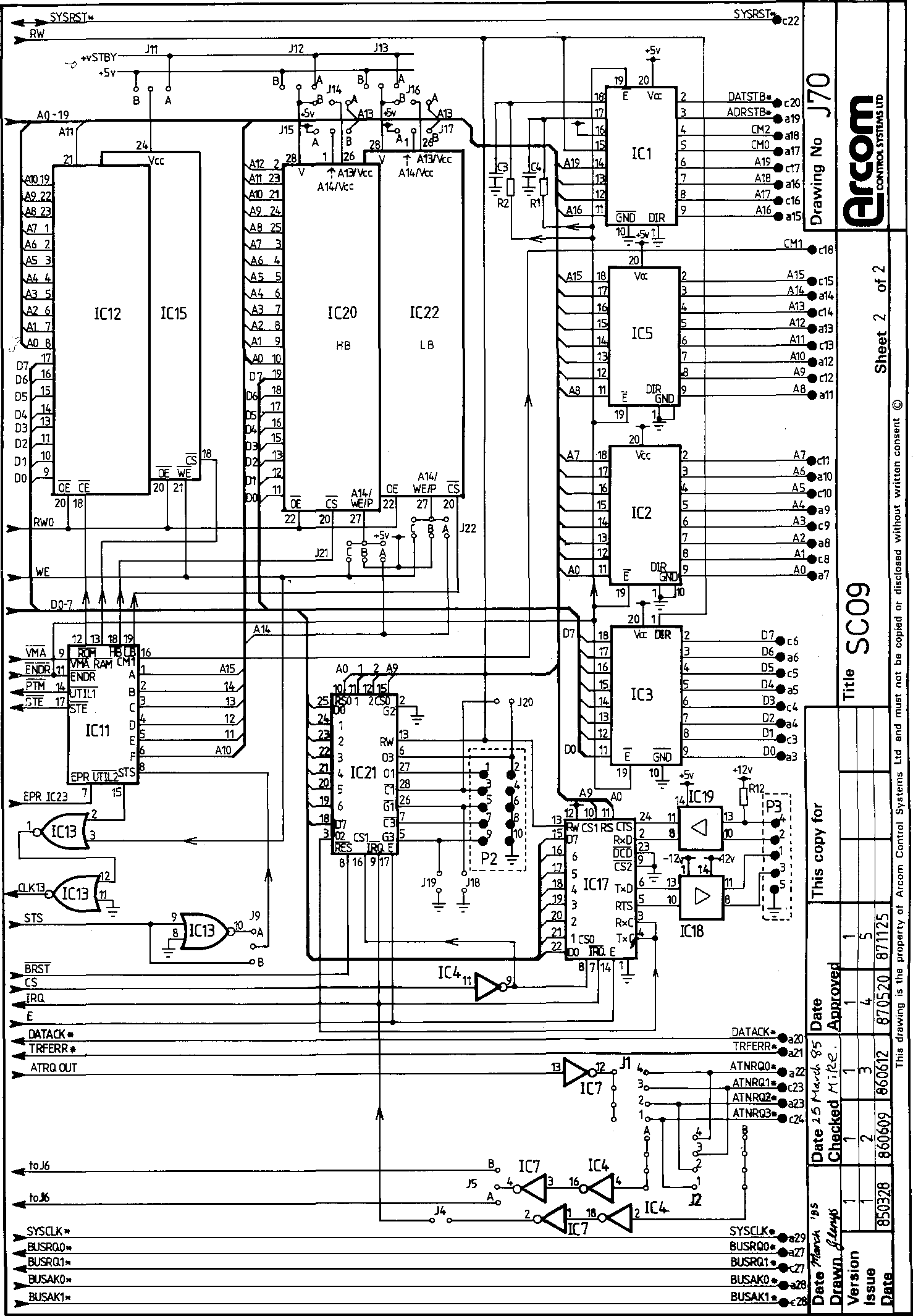
Passing on to Figure 6.26(b) of the circuit diagram, we notice four memory chips. IC12 is a 4K EPROM located at the top of memory, IC15 a 2K (6116) static RAM chip. The sizes of these chips would now be classed as small, but they are indicative of the date of design (1985). ICs 20 and 22 are RAM or EPROM chips (size 8K to 16K). IC11 is the memory map decoder PAL (16L8). This PAL also maps STEbus I/O locations into 6809 memory space - if a certain region of memory is accessed then the SC09 performs an STEbus cycle with CM1 LO (an I/O cycle). IC21 is a PTM (Programmable Timer Module, 6840), and IC17 is an ACIA (Asynchronous Communications Interface Adapter, 6850) or UART. ICs 18 and 19 drive and receive the RS-232 lines to and from the ACIA.
IC23 is a latch which stores the top four address lines, A16-19, for STEbus accesses, thereby extending the 6809’s address space from 64K to 1Mb. The latch also contains two control bits (EPR and STS) which modify the SC09’s memory map when set or cleared.
ICs 1, 2, 3 and 5 buffer data and address bus signals onto the STEbus. The buffers are enabled by the ENDR signal from IC10. ADRSTB* and DATSTB* are just this signal delayed by a resistor and capacitor to give the minimum 35 ns setup time required by the STEbus spec.
PAL IC9 contains the STEbus arbiter: BUSRQ0, 1* come in and cause IC9 to assert the 6809’s /HALT signal. When the 6809 has halted, as indicated by its BA and BS status signals, IC9 grants the STEbus to the appropriate requester. Notice that this means that the SC09 always acts in the default master mode and assumes it has control of the bus when it is running.

Figure 6.26a The SC09, a 6809 STEbus CPU board.

Figure 6.26b The SC09, sheet 2.
 Keith
Keith
Discussions
Become a Hackaday.io Member
Create an account to leave a comment. Already have an account? Log In.