A quick hand sketched schematic show there are only about 60 address + data + control connections, 25 power/ground, and about 15 hardware configuration connections. The address/data/control connections can be reduced to 30 if the RAM and flash are stacked together, piggy-back fashion, since so many RAM and flash signals have the same pin assignment and share the same connections.
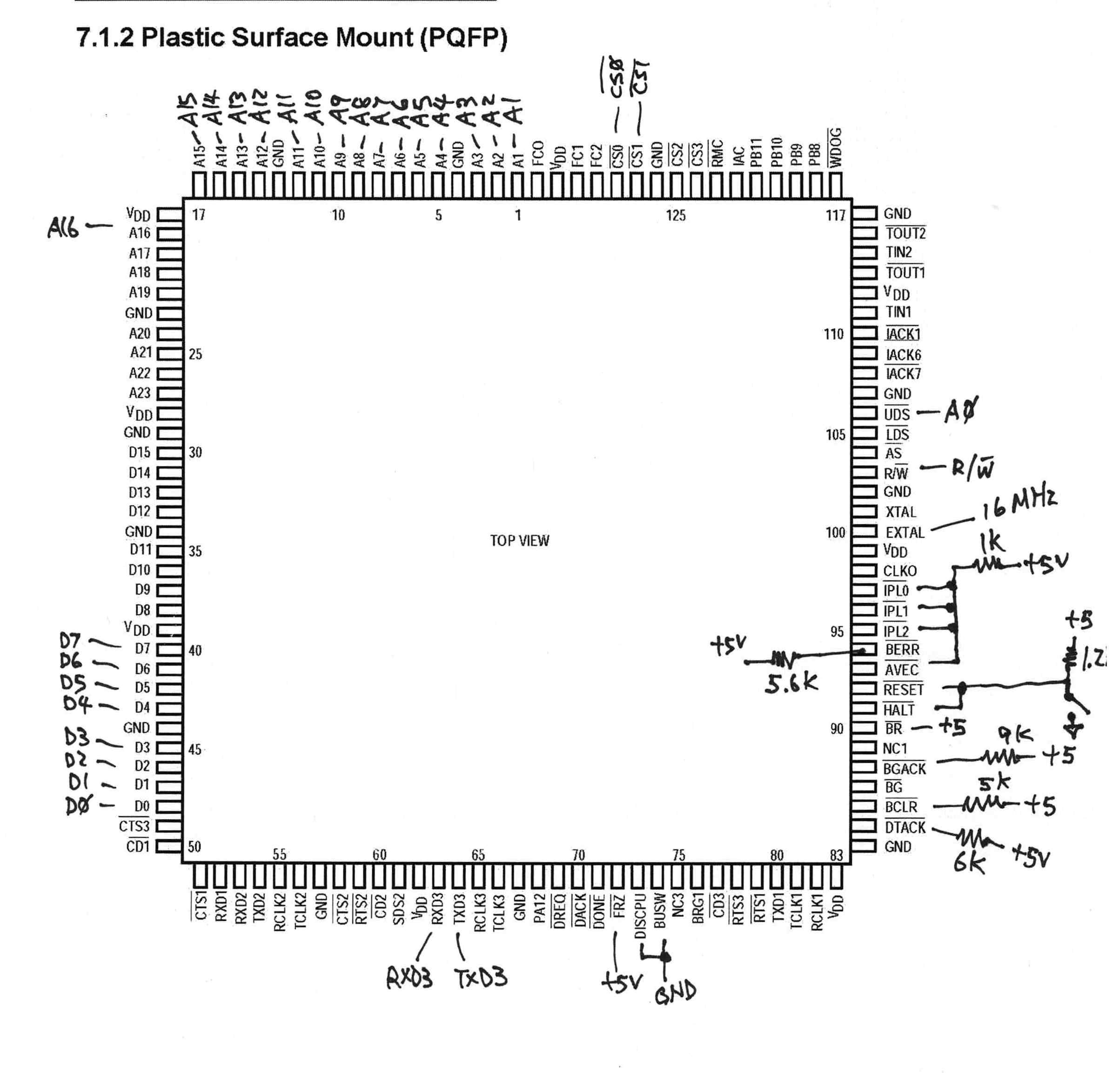
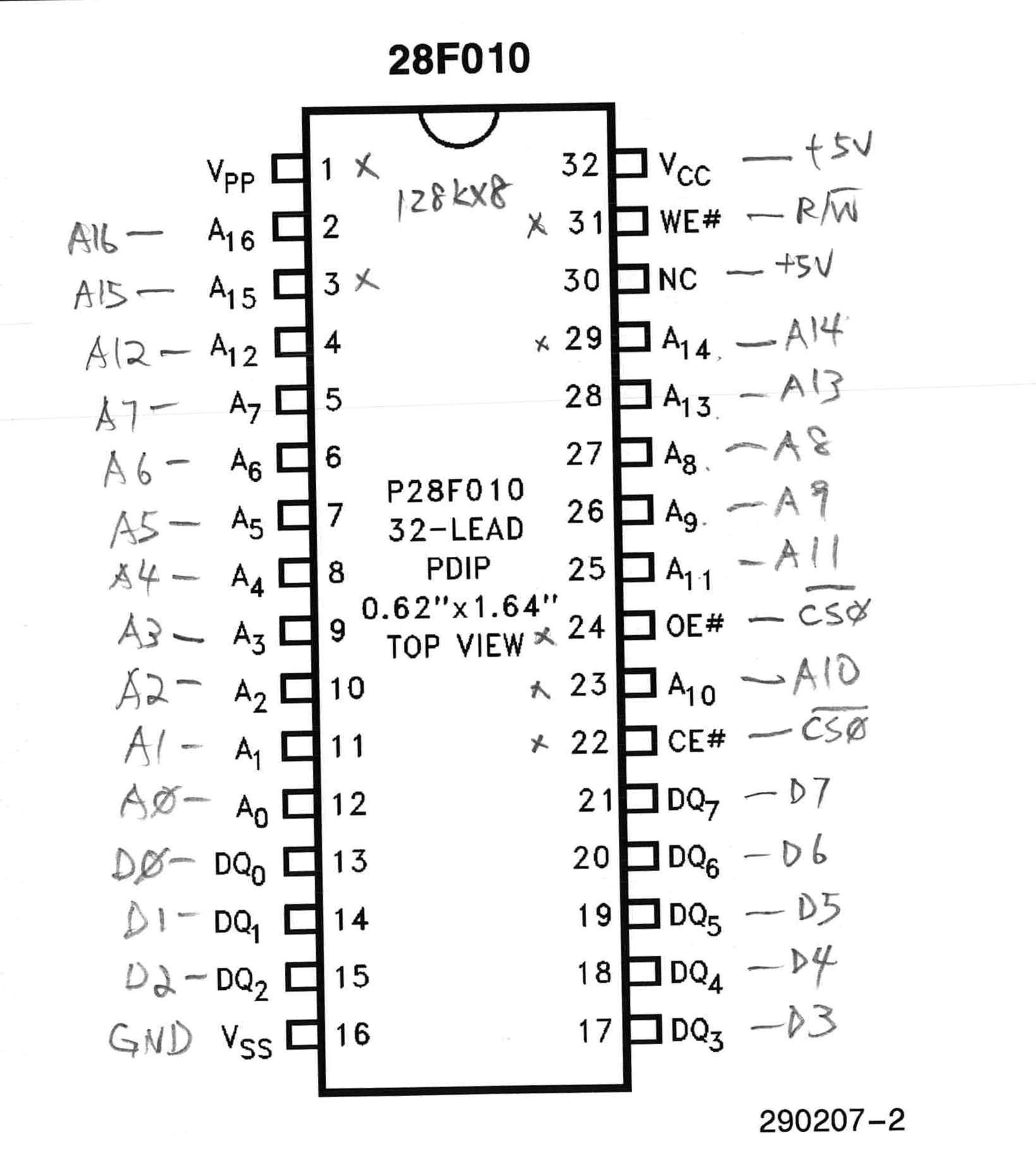
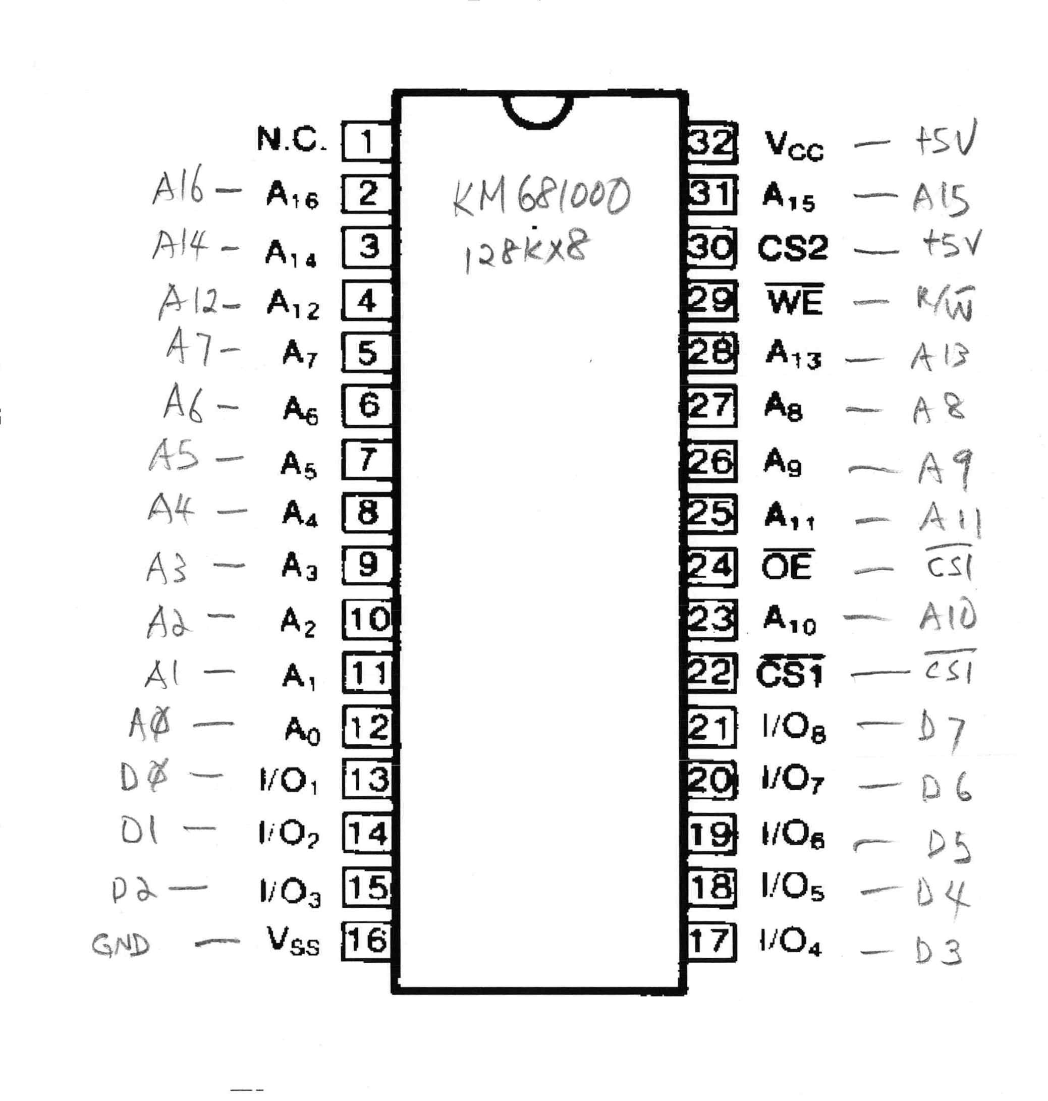
I have 128K RAM and flash in DIP package, but I don't have 68302 in PGA. You can buy them off eBay for under $20, but I thought I'll try with a quad flat pack 68302 that I removed from a 68302-based SPX-MPU board. (I removed all components so I can reverse engineer the pc board connections). The lead spacing of the QFP is 25 mil, so I have to work under a microscope and it will take more than an evening to wire 60 or so connections to the QFP.
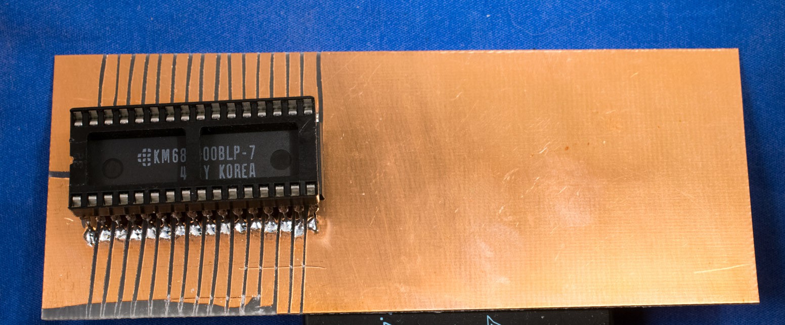
I want to have a solid digital ground, so all components are mounted on a single-sided 2"x5" copper board, copper foil up. Most of the copper foil is digital ground except areas carved out for other signals such as pads for the piggy-back RAM and flash. The piggy-back RAM/flash is soldered to the board because I need solid mechanical support to insert and remove the flash multiple times.
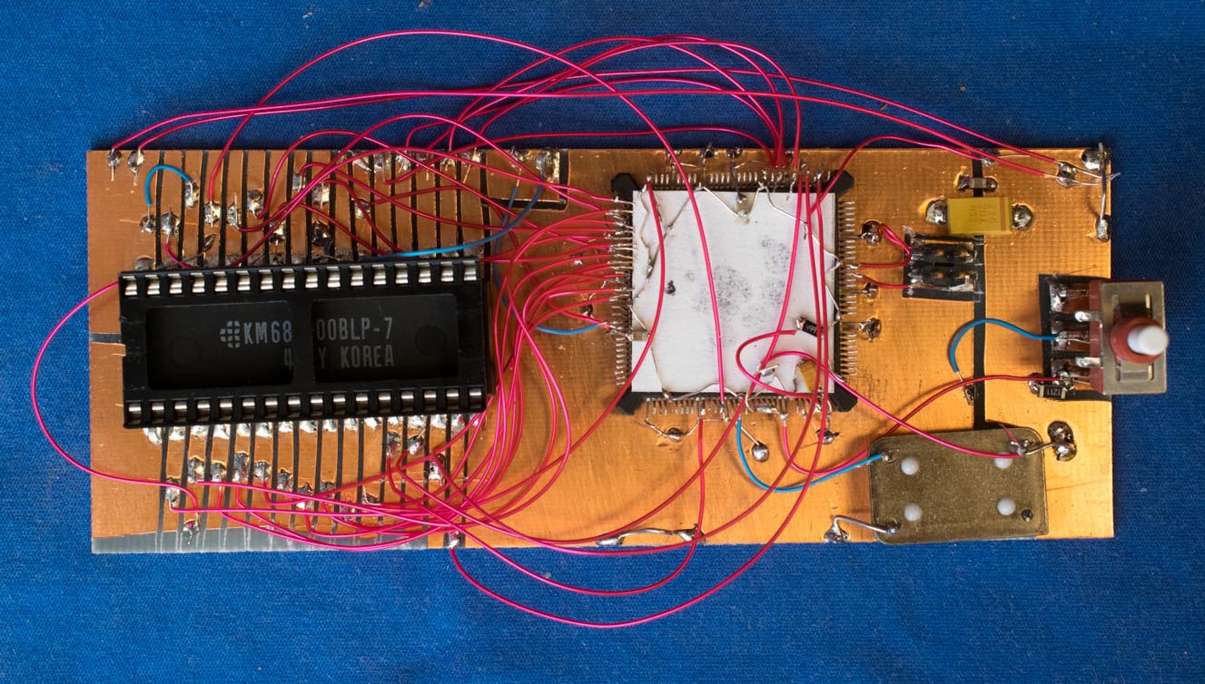
The QFP 68302 is glued to the board, dead-bug fashion. Ground leads are bent down toward the copper foil for short ground connections and Vcc leads bent toward the center where a 5V ring will be constructed. A third of way into wiring, after ground/power were connected and all hardware configuration finished, I connected the 16MHz oscillator and power up the CPU with oscillator. I can see chip select 0 puts out 8 successive pulses to fetch reset vector and system stack and repeat every 1 millisecond. That means the CPU is probably OK, even though I'd treated it rather badly when removing with a heat gun. Soldering 60 or so connection to the QFP 68302 was challenging and it did take more than an evening. I know I can do it 10 years ago and I'm glad I still can do it. Nevertheless I'll stick with the PGA package on the next iteration!
This is the finished board. It can fetch reset vector and execute an endless loop of NOP so flash is working. I'll need to test the RAM next and then bring up a simple bootloader.
 Plasmode
Discussions
Become a Hackaday.io Member
Create an account to leave a comment. Already have an account? Log In.