Close
0%
0%

Bench power supply

USB and manual control, and monitoring, 2 channel 5A 30V bench supply.

Similar projects worth following
Looking at the price of bench supplies got me thinking "I can do better", for much cheaper. digging around on ebay gave me lots of hope for ways to make this pretty quick and easy. I think all good projects come with lots of false hope, some finish only with excessive persistence.

The origional idea was to take some basic inexpensive parts from china and put them togethor to make a dual output bench supply. A primary converter from 120VAC to 35VDC is quite available, and small bucking modules from 32VDC to 0-30VDC are quite available. a few modifications and throw on some usb monitoring and or control and I'd have a nice new supply. Easy right?

Well, not quite. I'm building a full on 2 channel 5A 30V supply, 300w...

newpower.dxf

faceplate layout

VAR_PRODUCT_NAME-dxf - 31.41 kB - 01/13/2016 at 15:22

Download

View all 7 components

  • [a brief pause]

    Rue Mohr10/15/2022 at 04:39 0 comments

    The project is not abandoned! Did you know that switching power supplies have a LOT of little design details and they are REALLY fussy about you getting them right?

    Did you also know that the magnetic components they are made from a PURE EVIL and a whole aspect of science itself?? 

    I have learned a LOT since I had to put this project aside and the odds of me successfully finishing it have gone WAY UP since I paused work on it.

    Please keep standing by while we work out technical difficulties :]

  • Test power amp finished

    Rue Mohr02/03/2016 at 05:55 0 comments

    Kinda.

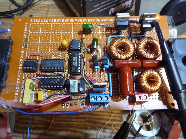
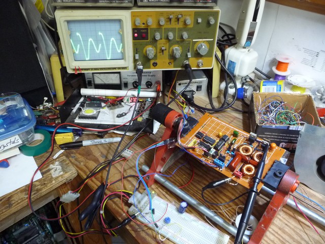
    I finished assembly of the low freq power amp. This is a ~40Khz, reduced voltage version of what I want for the final supply.

    And it works, but the disable line is backwards, it turns on both the drive transistors which shorts out the supply, oops. otherwise, less giving it a full load test, its working.

    If your wondering, the big green resistor is a part of a snubber circuit.

    The control circuit works well (less the disable, which, for now, I may just label 'self destruct') I have to back off the max drive duty as a slight delay in the transistors turning off causes them to buck heads just a bit.

    I'll work on connecting it to the regulator board and the current sense to see if I can get a power suppply out of it.

  • Rework of power amp... again

    Rue Mohr01/27/2016 at 10:26 0 comments

    So, I decided to build this 1 channel version of the power supply, and although I'm not directly documenting it, its research is going to be used in THIS power supply.

    What I did today: (its not tommorow till I'v slept)

    For the 1 channel supply I worked out I need a switching converter, this means building another one (the 250Khz one isn't going so hot) with whatever compromises are needed to just get it working. The goal for this one is to operate at about 40Khz.

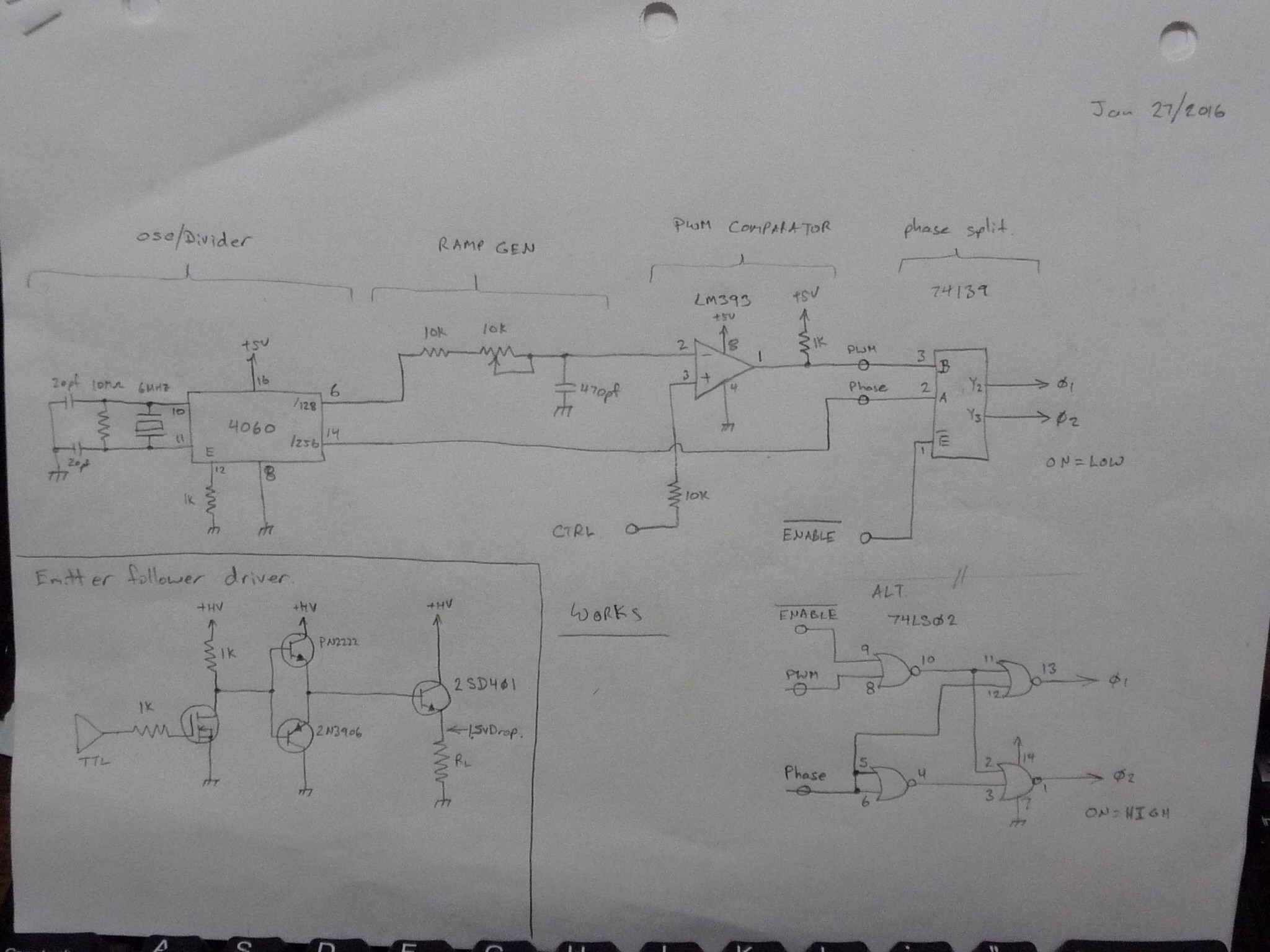
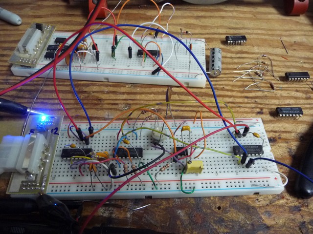
    Thinking on the pwm genorator schematic, I decided to try using a 4060 clock/divider chip, this would give me an oscillator and a divider all in one 16 pin package. (the last circuit took two, a 4069 for the osc and a 4013 for the dividers) As well, the 4060 has an array of dividers that would give me more options on the crystal I use.

    After pouring thru all my crystals and doing lots of division I worked out that the best option was a 6Mhz crystal with a divisor of 128 which gives me about 47Khz

    The pwm is generated in the same way as the last circuit, and while building it I noticed something interesting:

    ** If the LM393 is used with the ramp on pin 2 (-) and the control on pin 3 (+) its output is clean, BUT if you reverse the two pins (to, say invert the pwm) there is significant ringing on the output.

    This is probably what lead to some of the difficulties I was having with the previous circuits, my addition of the disable line required inverting the pwm, so I compensated for it at the comparitors inputs.

    --

    I decided to try something new with the phase splitting circuit, and I used a 74139. the TTL output it messy, but it does work. That said, when I started playing with driver circuits, I had to invert the outputs, and ended up using a circuit based on the 74LS02, which actually gave a much cleaner output.

    --

    Then I started playing with driver circuits. When I built the power board for this 'quick and dirty' supply, I used PNP transistors in common emitter mode.

    Playing with various configurations, I was unable to get any common emitter amplifiers to give a nice output, all of them had timing distortions at low duty. It seems in order to switch them off, you have to reverse bias the BE junction with atleast 1V.

    The idea struck that the common emitter amplifiers performance was SO terrible that I could probably get better output from a common collector amplifier, so I tried it...

    Its a bit laborious, you need to convert the ttl to full swing voltage, which I did with a 2N7000 and pullup resistor, and drive the base with some current, which I did with a PN2222/2N3906 totem pole pair. The output was GREAT, like, really great.

    It loses 1.5V from the supply rail to the load, thats equiv to a 0.3 Ohm mosfet at 5A, which is about where I'd be at by the time I found a P channel fet with a low enough input capacitance to use at high freq.

    --

    What did we learn today?

    Today we learned that capacitance really sucks!, weather its in an LM393 op-amp, or a power driver transistor, if you have an input that fighting with an inverted output, even 40Khz waveforms are going to suffer.

    I may change this quick and dirty supply to use a set of NPN transistors in common collector mode. I could use N channel fets in common drain, but I'd need a bias votlage about 5V higher than my top rail, which I CAN do }:], but I don't want to.

    Its 2:30am, goodnight.

    --

    oops funny what you miss at 2:30am, the output polarity is wrong,its supposed to go from 0-50% duty, need to redo that phase splitter as a NAND circuit :)

    more images:

  • Is it all worth it?

    Rue Mohr01/26/2016 at 06:31 0 comments

    So, in a move of "hey lets do something crazy to get soemthing working here" I decided to detour on a spinoff project and makea lower voltage, 1 channel version of this supply using a Dell power supply and a linear regulator stage.

    The dell supply can put out "6.7A" at 19.5V, I wanted to test if it could sustain much of any power so I broke out my linear load bank and had it slowly dial up to 5A (which is its limit, damn me for using a 1 ohm feedback resistor and a 0-5V refernce) It took the 5A fine, so I decided to do a time test for a modest 3A over a 20 mins period or so and see if the adapter heated up at all. about 5 minutes into the process I checked the adapter and its temp was ok, a bit warm but nothing significant. then I touched the load bank to make sure it was ok, and it was burning hot.

    My load bank uses a large heatsink, about 48inch^2, with fins, the heatsink I had slated for the power supply was about 8 inch^2. This is a problem, if my large heatsink couldn't handle 60W continious, the heatsink for the power supply, operated in linear mode wouldn't have a chance.

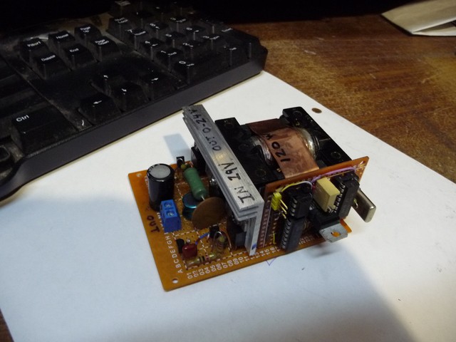
    So, yes, I need to use a switching converter.

    I assembled a quick and dirty pushpull converter for it that should be able to take up to 150W, only designed to operate at about 40Khz, and even put some extra turns on it so that I can get 24V output. so quick it uses PNP bipolar transistors. Now, I need a pwm controller, has to be 2 phase cause its operating a pushpull. I decided to take a closer look at the TL494, which is starting to look a lot like the circuit I developed for the amin project here. Cheating it, to make it operate as a pwm genorator, I'm able to drive in voltage and get an output duty from 0% to 78%, and thats all she wrote. The TL494 cant go over 78%.

    That is just like having dropout on a regulator. If I wanted to have an output of, for example 10V, I'd need about 13V going in, and thats not accounting for transistor or diode loss (which put it up to about 15.3V) My converter goes from 0-100%

    ok, so far I'm on the right track. sometimes it just dosn't feel like it.

  • Less is more.

    Rue Mohr01/18/2016 at 07:00 0 comments

    No, I'm not talking linux command line utilities, I'm talking mosfets. I'm still not too happy with how the mosfets are switching, in the process of trying to confirm a new power filter, I'v been playing with mosfet drivers. Go figure, it turns out that really big mosfets just dont switch nicely, its not about the gate capacitance to the source, its about the capacitance beween the gate and the drain.

    This is a common source amplifer, because of that, its output is inverted. As the gate votlage goes (talking about P channel here) down, the drain voltage goes up, the capacitive coupling between the gate and drain causes the rising output to cancel the efforts of the FET driver, which causes a stall or even reverse of the gate voltage change.

    I used moderatly large capacity fets in my design to try to bring down the Rdson, but I think I went too far, there is a point where the fet is so large that its combined capacitances cant be well driven at high frequencies.

    My power supply is just 5A, I was playing with some 20V, "75A " fets (much smaller) that were switching much nicer at 250Khz, even at 40Khz you can see a difference.

    oh, and with a filter of two stages at 220uH and 47uF I get about 10mv ripple out.

    Another side note, you really have to watch were you ground the scope, with switching like this ground voltages stack up fast. If you watch a few episodes of the EEV blog, you will notice him write off the HF chips in his scope readings. most of it really is artifacts from probing the circuit, quantum finish.

  • Opps, thats gonna need math.

    Rue Mohr01/14/2016 at 05:00 0 comments

    I just finished assembly of the power board and found out that stage 1 of the output filter resonates at 222.2Khz (the converter runs at 227.5Khz) so I'll have to redesign the output filter.

    looka me! I made a resonance converter!

    Aside from that everything looks good.

  • CMOS to the rescue!

    Rue Mohr01/12/2016 at 06:58 0 comments

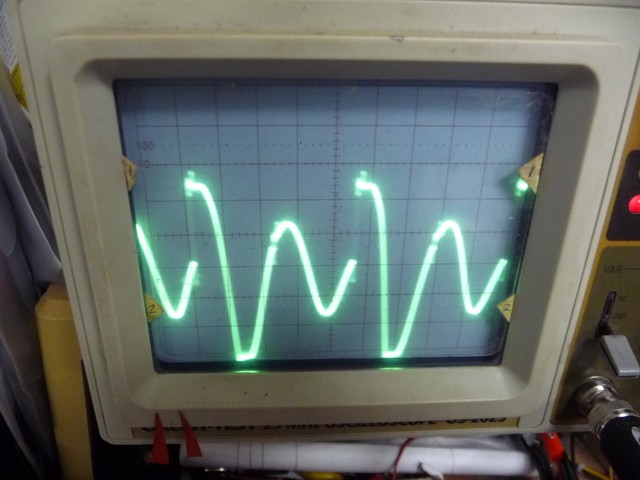
    So, I been wrestling for quite a while with the pwm genorator trying to get rid of little glitches and bounces and ringing that came up during final assembly. The final straw was a 40mv, 5Mhz ring that caused the pwm comparitor to output a ring that the driver would pick up on. In the process I found out that as the control input votlage got close to 100%, the oscillator would change freq and slip thru another glitch that would double clock the flipflop causing th pwm to be split up wrong.

    ARGKGH.

    Has to be another way.

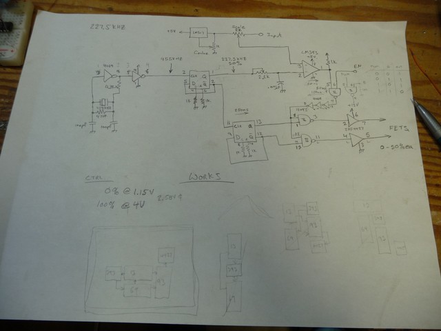
    Sitting down and thinking, an idea occured. my origional design uses a ramping oscillator to also generate a square wave. What if I did this the other way around, took a nice reliable square wave genorator, and put it thru a RC filter to generate a ramp. its much easier to generate a stable stable square wave osc, I could use a 1 MHz crystal and divide it down to the 250Khz.

    It also occurred to me that I had some low freq ceramic resonators, possibly one perfect for the job.

    455Khz, is a common one, /2 = 227.5Khz, which is close enough to my 250Khz smps goal. quite a bit of the problems from the origional design were caused by the overshooting of the TTL logic gates, this is fine for a digital circuit, but this circuit is a hybrid.

    CMOS to the rescue, its slower, its transitions are underdamped, and so its less noisy, no 5Mhz ringing.

    The basic theme is the same, there is a osc that outputs a square wave and a ramp, the ramp is fed into a pwm comparitor, the square wave divies up the pwm into two channels that go to a driver.

    Its assembled and it works great. In the process I had two surprises.

    1) The input of the LM393 draws a "LOT" of current when it crosses over its threashold, enough to throw out high impedence input signals, this is what was causing the osc in the origional circuit to freak out.

    2) propigation delay. I actually had to add 3 inverters in the circuit to make up 150ns of delay and align signals, never had to do that with a circuit before.

    It turns out this is a nice circuit, by adjusting the resistor on the RC, you can trim the amplitude of the pwm ramp. I put an offset and scale control on the main input to help match the two siganls.

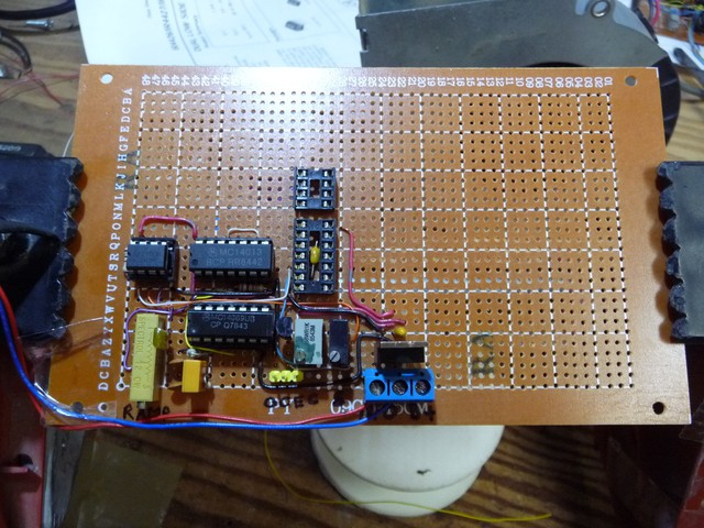
    New veroboard, start again,

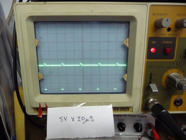
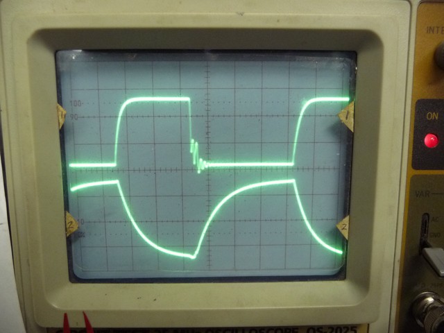
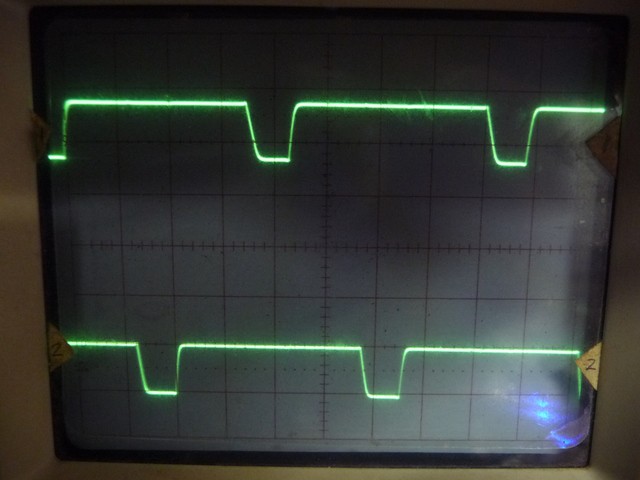
    (old pic) its finished, the outputs look great. I get from 0-100% between the two channels with NO little glitches anywhere thru the duty sweep.

    I'm just re-assembling my fet driver (post driver chip) to make sure its good with the driver chip and I can finish the power converter.

    YAY!

    But the question arises, could I have used two syncronized 3842 open loop to generate the pwm? [hint: its too late to ask this question]

  • If you can beat 'em, meet 'em

    Rue Mohr12/22/2015 at 06:18 0 comments

    ok I ordered fet drivers, I'm testing, please stand by.

    Jan 7/2016

    --

    So it turns out that a 555 is a GREAT fet driver IF you have the input levels at EXACTLY the right bias and amplitude, slightly off and the duty of the signal your driving goes really, really wrong. so I bought some official fet drivers. IRF4427.

    I'v recieved the drivers and they seem to drive the fets ok, as good as, or a little better than the 555 was.

    One of the other problems thats come up since I breadboarded this circuit is that there is a 0.2us, 5Mhz, .02V 'ring' in the ramp signal where it crosses the threshold votlage of the control signal. For the most part this dosn't cause a problem, untill the control voltage is close to the peaks of the ramp, at which point it causes a brief glitch in the pwm comparitor output, which is then amplified by all the stages and comes out quite clearly on the output of the fet driver.

    I'm looking at two methods of fixing this,

    a) drop 1.4V off the comparitor output. The spike, at the output of the pwm comparitor, is only about 0.7V, much less than the 5V of the rest of the pwm signal.

    b) new ramp oscillator circuit.... again? really?

    welcome to 2016 everyone!

  • Assembly of the power stage.

    Rue Mohr11/24/2015 at 05:06 0 comments

    Nov 23:

    I'v started assembling the PWM power converter. During which I realized that when I modified pwm genorator to run on 5V, it was in part to make it match the error amplifier output, that whole transistor stage on the end of the error amp isn't needed anymore. oops.

    So far, the pwm genorator is working. With luck, over the next few days, I'll get the schmitt, phase splitter, and fet driver going.

    Nov 24:

    Dear diary...

    I assembled the rest of the phase splitter circuit and found some interesting problems, this isn't supposed to happen cause I'v already tested these circuits.

    A glitch pulse in the pwm comparitor caused the pulses in the toggle flip-flop to get all messed up, After a lot of probing I found that I needed to add a 22pf cap between two of the ramp genorator pins, I'm going to attribute this to making up for the breadboard capacitance I dont have anymore.

    It was then followed by an interesting timing error in the division of the pwm. The T flipflop is supposed to redirect the pwm signal after its definitly finished a cycle, this switching is happening a bit early and breaking up the pwm cycle wrong. In the process of trying to correct this, the ramp oscillator stopped working.

    Thats as far as I got, I'm going to sit back and see if I can make some changes to garuntee better operation., like clocking the T flipflop off the pwm itself.... thats a good one... better write that down...

  • Buck smps filter.

    Rue Mohr11/15/2015 at 21:10 0 comments

    This is the big evil, the LC filter for the buck converter. I had really hoped to stay away from assembling a full blown set of drivers to test the filter, but the freq gen I have cant drive the power fet directly. arg.

    I assembled the 5V driver I'd worked out before, with a 50% 250Khz source from the frequency gen and started to test, it didn't take long to work out that the 5V drive to the power fet will not work out. And so came a new problem, new power fet driver.

    I tried LOTS of fet driver designs, and the result was halarious.

    There are two parts to the problem, the pwm needs to be taken from 5V levels to 12V levels, then current amplified to drive the fet at 250Khz, with desired switching times of 0.1us, this isn't easy.

    The origional driver I designed just drove the fet at 5V, so I didn't have to worry about stepping up the voltage. My first circuits to step up the votlage were transistor based first bipolar and then fet (2N7000), niether of those yeilded good results (lots of ringing and skew that would not go away.)

    So I tried an LM393 for stepping up the votlage, with a bipolar totem for driving the problem was that the bipolar totem would ring badly,

    So then I tried a small fet totem pole, which I ran into a new problem, the lm393 can only drive 20mA, and that dosn't work with the 300pf input capacitance of them (AOP605)

    So I stood back and thought,

    click* a 555 is a 12V capable latched window coparitor with a totem pole output driver thats rated at... 300mA! (the 300pF needs about 30mA to get 0.1us switching across 10V)

    However, as it turns out, the output is sufficient to drive the main fet directly, I dont even need an extra current driver.

    LM555,

    Pin 8 to +12V, pin 1 to ground,

    Tie 2,6 togethor, thats the 5V logic level input.

    Tie pin 5 to ground via a 1k resistor, this brings the threshold of the inputs to 5V levels.

    pin 4 (reset) gets tied high (pin 8)

    pin 3 is output to fet. (I use a series 10-100 ohms resistor)

    Its too bad the 555 cant be used to generate the 0-100% duty pwm.

    oh yea the fitler. The design looks good, the first stage filters the noise to 0.6V, the second stage takes out everything else.

    There are still things that could be improved, for sure if I just dialed the converter freq down to 40Khz or so, I'd have a great circuit. or even 80k, even 160k....

    This is how I stay up till 4:30am

    --.

    Today I worked on it a but more,

    There is an almost inpercievable difference between the 555 output running the power fet directly and inserting a bipolar totem pole driver. I was able to improve the switching by inserting a diode across the gate resistor to hurry up the turnoff time, and I was able to quench some of the ringing the power fet generates with a ferrite bead on the Source pin.

    Turnon is less than 0.1us and turnoff is about 1.5us

    --.

    So, while trying to test the filter, I realized a failure point, I put one of the inductor cores I'm planning to use and ran 5A thru it continious, it got WAY too hot. At the same time, I'v worked out that I dont need anything close to the 2uH I was planning on using,, this means I can dial down the turns on the inductor and bring down the resistance, which will help. I'll work this out more with a working pwm genorator.

View all 33 project logs

  • 1
    Step 1

    1) Come up with a simple good idea.

    2) Add good ideas to it.

    3) Try to implement it.

    4) When it fails, start to strip down the design to try to get it to work.

    5) Strip it down more

    6) More...

    7) Rejoyce when something simple works

    8) Add a few simple things to it.

    9) Give up getting it working with anymore than the basics.

    10) Put it in a box.

    11) Take it out and make it work again.

    12) Box it back up.

    13) Reassmble with one screw missing.

    14) Be happy with whats left.

View all instructions

Enjoy this project?

Share

Discussions

Rue Mohr wrote 08/28/2014 at 08:45 point
thanks, I'm still wrestling with the regualtor design, I have something working, but the output ripple is .2V, I'm aiming at .05V

  Are you sure? yes | no

Ron wrote 07/01/2014 at 22:00 point
Nice Power Supply

  Are you sure? yes | no

Similar Projects

Does this project spark your interest?

Become a member to follow this project and never miss any updates