Close
0%
0%

ZX81 hi-res graphics board G007

By Gary Keall. 256x192 pixels.
Patches BASIC so you can PLOT(n,x,y)
instead of USR(addr) calls.

Similar projects worth following
Other graphics boards require many USR() statements to execute machine-code routines.
This board patches the ROM to change the BASIC language, which makes it very easy to use.
I have added 32K static RAM to my board, to reduce the number of wobbly connections and allow the use of a single 5V power supply.

This amazing upgrade belies the enormous amount of cleverness packing the functionality into a handful of TTL chips and a tiny 2K EPROM. It has been integrated into a ZX81 emulator if you want to try it out!

The circuit diagram is from the Maplin magazine issue.

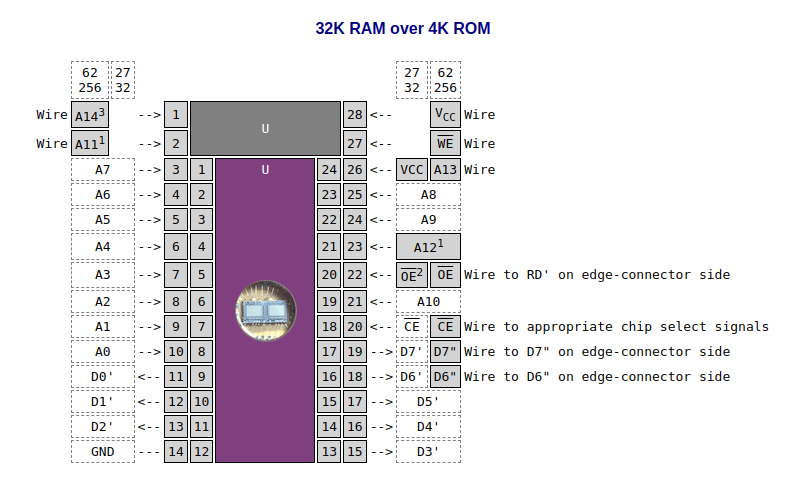
The board I have was a kind and generous gift from the designer, and differs from the Maplin circuit. It uses a 74LS125 chip instead of a 74LS03 for IC3, and a 74LS02 instead of a 74LS32 for IC6. This allows it to work with just one pull-up resistor instead of two. My board has some of the gates swapped, which is important when adding hacks to it.

I pulled the parts off to record the PCB tracks under the chips, and to socket the chips so I could partly replace them with PAL chips. Alas, this has caused it to stop working! :-(

Removing a short circuit allowed the piggy-pack RAM to work again, but hasn't got the graphics working again. I don't know whether to bother repairing this one or getting some new boards made. We know the circuit works, and the RAM chip circuit works, so it is not risking a load of dud boards.

G007-1.EQN.TXT

First draft PAL equations. Compiles, but untested.

plain - 3.83 kB - 10/28/2025 at 00:20

Download

PCW 1983-03 Article G007 GRAPHICS MODULE.zip

Personal Computer World review, converted to html form,

Zip Archive - 227.45 kB - 10/25/2025 at 15:44

Download

G007-non-Maplin-analysis-2nd-draft.pdf

Made by editing the original non-KiCad CAD file. A lot of reverse engineering done.

Adobe Portable Document Format - 65.38 kB - 10/25/2025 at 00:56

Preview

G007-non-Maplin-analysis-1st-draft.pdf

KiCad sketch of my non-Maplin version of the board. Not checked yet, but you can see the differences.

Adobe Portable Document Format - 105.52 kB - 10/24/2025 at 01:03

Preview

Ritger,Wilf.zip

Wilf Ritger's articles about the ZX81 video, in German and English HTML.

Zip Archive - 43.67 kB - 10/07/2023 at 03:03

Download

View all 12 files

  • Migrating TTL to programmable logic

    Keith10/27/2025 at 01:21 0 comments

    I want to do this to gain:

    • Logic equations that can be added to CPLD/FPGA versions of the ZX81. 
    • Clearer understanding of how it works
    • An easily modifiable version
    • Ability to add features

    So far, I can see

    • The video data is clocked into an 8-bit latch outside refresh cycles
    • The video data is read from the latch during refresh cycles and graphics mode is on
    • The ZX81 ULA considers any video character with D7 and D6 low to be a 'NOP'
    • The G007 forces D7 and D6 low when fetching opcodes and A15=1 (i.e. fetching video data)
    • The ZX81 ROM has a 256-byte patch of ROM at 0Cxx and RAM patches  at  02xx and 22xx
    • The ZX81 RAM is enabled at 2000-27FF, AND at the RAM patches in graphics mode
    • The ZX81 ROM is enabled at 0000-1FFF, disabled at the ROM patch, and at the RAM patches in graphics mode
    • The G007 RAM is enabled at 2800-2FFF, AND at the RAM patches in graphics mode
    • The G007 ROM is enabled at 3000-37FF, AND at the ROM patch
    • The video data latch is read during refresh cycles when graphics mode is on
    • All memories are disabled when the G007 is driving D7 and D6 low, or reading the video latch
    • Off-board memory read data is enabled when the G007 is not driving D7 and D6 low

    The last point is only for memory access. The buffers are not enabled for I/O access, which might explain why the printer must go between the ZX81 and the G007 board. The programmable logic might be able to allow I/O access through the G007.

    I asked the designer why not just switch between two versions of the 8K BASIC ROM. This would be simpler than all the patching logic. He said this was true but would require a 16K ROM and Sinclair might object to having almost his entire ROM copied.

    Another point is that the RAM patches allow you to add further values of n to the PLOT n,x,y commands. Currently n is up to 130 but you could add commands for ellipses, curves etc. If you have the time to write that code!

    These days, memory costs are insignificant and Sinclair unlikely to litigate for loss of income. You might actually need a whole new ROM for modified ZX81 firmware (e.g. square pixel clock rates, or the Shoulders of Giants bug fixed ROM).

    However, I'm just going to start with the original design before I try adding any enhancements.

    I am using the Opal software suite, mostly the EQN2JED command. I found some unusual behaviours. In other PAL compilers, you can do something like this:

    a = b * c
    d = e * f
    g = a * d

    but EQN2PAL complains. I now have to do this:

    @define a " b * c "
    @define d " e * f "
    g = a * d

    This works in a very simplistic string substitution fashion. It will not convert complicated expressions into equivalents. 

    Another issue is that where some logic compilers understand defining GND = 12 and VCC=24, the EQU2JED thinks you are defining output terms. Which is fine until you reach 9 real outputs of a 22V10 chip and EQN2JED complains about your 9th real term. Even though there is nothing wrong with it. It thinks it is your 11th output term, which is more than a 22V10 has. Commenting out the power and ground pins fixes this issue.

  • Hacking a 16K SRAM pack

    Keith01/20/2024 at 20:16 0 comments

    I bought a 16K SRAM pack from https://www.youmakerobots.com/sinclair/85-zx81-16k-ram-kit.html on eBay for £18.

    It uses this circuit:

    I assembled this and it worked fine.

    The board can be modified to provide the full 32K of the RAM chip by driving RAM pin A14 from /M1 * A15.
    This forces RAM A14 low when "running" the display.
    The ram at $C000 to $FFFF is now not an alias of the user RAM but an extra 16K RAM that can be read and written to, but machine-code cannot be run there.
    The right-hand pair of NAND gates in the LS00 chip have floating pins, which is a bit naughty but you can get away with it with TTL chips. Having floating pins makes the 32K modification easy, because the pins can be simply wired up.
    The RAM A14 pin is grounded, but thankfully has thermal breaks so you only need to cut four small PCB tracks.

    A further mod would allow you to relocate the ZX81's on-board RAM. Maybe not worth it for just 1K (although the G007 board uses it). However, if you have up to 8K you could re-map that at $1000-$1FFFF. Or re-map bigger memories to $8000-$BFFF as well. Such mods would require more logic than this 16K RAM board has available.

  • Background reading

    Keith10/07/2023 at 02:45 0 comments

    The basic principles of ZX video are fairly simple but there are many details that I'd rather not have to learn.

    Someone who does fully understand ZX81 video - the remarkable Andy Rea - pointed me to articles written by an earlier expert, Wilf Rigter, in the ZXirQLiveAlive magazine:

    Vol 6 No 4 page 19 (part 1)

    Vol 7 No 1 page n27 (part 2)

    Vol 10 No 3 page 7 (part 4)

    Googling around, I found it in HTML (and German) and got Chrome to translate it. This gives a more readable form than the scanned magazine articles. There are a few errors such as figure numbers so I polished it up to my own style.

    I've learned some interesting tricks that I'd like to incorporate into my own future designs. 

    • A normal 16K DRAM expansion appears when A14 is high and as a non-executable alias when A15 is high, which is fine when you have just 16K. If you have a 32K RAM expansion, half is usually wasted by tying A14 high or low. A handy and easy mod is to feed A15 and /M1 into an AND gate and wiring the result to A14 of the 32K RAM. Two diodes and a pull-up resistor will do. This means the CPU will get bytes from the lower half when it 'executes' the display file, but can read and write data to the upper half.  You can't run machine code there, but you have 16K for storing data.
    • Normal ZX80/81 logic forces a nop code whenever A15 is high. If you are recreating a ZX80/81, you can limit this to the last 16K (A15 and A14 high). You can then run machine code between 32K and 48K.
    • The hi-res graphics methods in the article involve ANDing the /RD signal with /RFSH and feeding the result to the RAM. This reads the RAM during refresh cycles as well as the usual read cycles. 
      It also ties the /RFSH pin of the RAM expansion high, which prevents any refresh cycles happening on dynamic RAM boards. You are probably limited to static RAM expansion. 
    • The address lines are driven by the I and R registers, so each video line has to execute a row of NOP codes while the I and R registers point to an "H-file".
    • The G007 was designed to not need mods, the LS374 latch is there to store the bus data when a video byte "opcode" is read, and then present it to the bus during the refresh pulse when the shift register is being loaded. The address lines are driven by the program counter, using a "D-file" in a similar way as low-res video.
    • The G007 method seems the best, but I'd like to be able to support both methods if possible, because there are many old programs using the Wilf Rigter method.
    • Comparing the G007 and ZX80 logic looking for common circuitry, I can see a couple.
      • The signal that latches the video byte is identical: MREQ & /RFSH * /CLK
        and it latches the data at the end of T2.
        I think it could work with just the rising edge of /RD or /M1. The ZX81+38 circuit uses /RD. Signal /M1 happens less often than /RD and thus generate less RF noise, but /RD rises sooner.
      • The signal selecting the latch output is /RFSH on the ZX80, and /RFSH during high-res graphics mode.
      • D7 and D7 are forced low when high-res graphics mode, A15 high, and /M1 low.
        It looks like G007 U7A, U9A, U1B and U1C exist just to prevent the expansion memory board D7 and D6 from being pulled low. I thought I could do Sinclair's trick of using resistors to limit the conflict (resistorplexing?), but there are already resistors in the D7/D6 signal path. If I'm integrating the G007 logic into the ZX81 logic, maybe I could pull D7 and D6 low at the CPU side of the resistors and then omit the isolation circuitry.
    • Most of the circuit does the memory patching. If using a pre-patched ROM, maybe this can be omitted?

  • Parts list

    Keith10/05/2023 at 00:50 0 comments

    For the Maplin version

    Resistors

    All 0.4 W 1% metal film

    R1,2   1k0        2 off    

    Capacitors

    C1-3   10n disc    3 off    

    Seems a bit small. I'd fit 100n capacitors. And a 22u electrolytic.

    Semiconductors

    IC1    74LS126           *
    IC2    74LS04            
    IC3    74LS03            is 74LS125 on my board
    IC4    74LS11            
    IC5    74LS00            
    IC6    74LS32            is 74LS02 on my board
    IC7    74LS27            
    IC8    74LS260           
    IC9    74LS74            
    IC10   74LS374           
    IC11   2716(M8)          

    Miscellaneous

    P.C. Board
    Track pin 5 packets 
    Socket 24 Pin DIL
    Socket 2×23 way 
    P.C. Edge connector

  • Upgrading to 32K EEPROM

    Keith09/16/2023 at 16:39 0 comments

    2023-09-16 

    This has to be done on the motherboard, where it doubles as the character font generator.

    Note that pin 1 is on a wide 5V track, and fiddly to isolate. I've just put my code in both halves of the 28C256.

    As mentioned elsewhere, the G007 board 'patches' the ZX81 BASIC to change the syntax of graphics commands.

    I suspect this could be done more easily by having a ROM with two copies of BASIC, one as normal and one pre-modified. The patching logic could then be removed. However, this would have two problems back in 1982.

    Firstly, much of the new ROM would be Sinclair code, and thus open to litigation.

    Secondly, memory was more expensive back then. In December 1983 when the Maplin article was published, UK prices in Electronics Today International February 1983 were:

    2716 £2.79 (£11.73)
    2732 £2.99 (£12.57)
    2764 £9.99 (£41.99)

    (2023 equivalent price in brackets)

    I can't even seen a 27128 or 27256 in that issue, but even if the price was directly proportional to size,
    then 20 or 40 pounds then would be the equivalent of 84 or 168 pounds in 2023.

    In 2023, one can now buy a 32K EEPROM for about £11, equivalent to the price of a 2716 in 1983.
    So price isn't an issue and Sinclair no longer exists.

    2023-09-25

    It also occured to me that the code in the 'shoulders of giants' version may be so different from the original that the ROM patching does not match, and thus fails.

    So I decided to get the latest official ZX81 ROM (version 3) and compare the patched areas with the original. I found out I had done this way back in 2011-05-02.

    Only 17 bytes are modified in the RAM patches. There are some differences at 07FD, 083E and 0843 which I wasn't expecting. I thought the ROM patch was at 0C00 and 2C00. Maybe the emulator used a very different board? This will need checking out.

    I've uploaded the files I have created so far.

  • Getting it working again

    Keith09/09/2023 at 21:47 0 comments

    2023-09-09

    For some reason, it isn't working. The 32K RAM piggy-back is working, but graphics are not.

    It has been modified to take a 4K EPROM.

    Quick tests:

    1 LET B=11520
    10 FOR A = 0 TO 8
    20 PRINT PEEK A - PEEK (B+A)
    30 NEXT A

     I get:

    128
    64
    32
    16
    8
    4
    2
    1

     This is what I expect, indicating the G007 ROM is present.

    But looking at 8192 onward, all I see is 255 when I expect random RAM values. Okay, they might be 255 by chance but POKE 8192,55 does not change the value returned by PEEK.

    I deduce that the G007 ROM is present but the 2K RAM that should be at 8192, is not.

    There should be a monitor I can use. The original article said:

    9996 STOP
    9997 POKE 16417, 0
    9998 RAND USR 32598; REM 7F56
    9999 GOTO 9996

    So the new entry point should be 32598 - 16384 = 16214

    RAND USR 16214

    crashes my system. I suspect the monitor RAM is not there either.

    Tracing back the ZX81 /RAMCS signal from the 8K RAM pin 20, edge connector contact 2A, pin 11 of U5 gate D. A11 used to select G007 ROM/RAM. A11 is edge connector pad 1B. Seems fine, maybe ZX81 RAM is only present if in graphics mode, and the ROM is not letting it do that.

    I notice that my board differs from the Maplin circuit again, as U6 is a NOR gate instead of an LS32 OR gate. I really ought to work out the circuit diagram for it.

    2023-09-12

    The ROM patch is always present when the G007 board is fitted, so the design could be simplified by having a ready-patched BASIC. As a bonus, the 256 byte patch is freed for other uses.

    I noticed that the ZX80 circuit does not have the ROM chip select taken through a resistor to pad 23B, as it is on the ZX81.
    This explains why my ZX80 was not accepting G007 commands. The BASIC ROM was simply not being patched.

    I went to mod my modern board when I noticed it does have this feature but only if you make jumper 99. So I did.

    I now find I when I type in lines of BASIC, it now crashes after pressing NEWLINE.

    Clearly the BASIC ROM is now being patched, but badly! Oh well, it is a step in the right direction.

    2023-09-14

    I found the numerous non-connections between the ROM and RAM chip data lines were due to most of them being swapped around. And the Z80 was not fully seated in its socket. So I pressed the Z80 down and ... it still isn't working. Checked the ROM socket modified for EEPROM - found /WE floating. Tied this high. Something poorly visible on screen. Adjusted TV from white-on-black to black-on-white levels. Hurrah! it works!

    I know the 32K RAM circuit works when the ZX81 /ROMCS is not connected, so I think the problems are now just down to the G007 ROM patching circuitry. My board circuit differs from the Maplin version, so I will have to reverse engineer it before proceeding.

    2023-09-26

    It is possible that the G007 board is not compatible with the heavily corrected 'shoulders of giants' version of ZX81 BASIC so to remove this possibility I created a reference ROM with ZX BASIC edition 3 at location 0000. It is a 32K EEPROM, so in the second half I have put the same BASIC ready-patched with G007 firmware, plus the 2K G007 ROM and a 2K monitor.

    This ROM boots up to a stable cursor. I'd like to do more but the plastic film keypad broke. So the next job is to wire up my new PCB keyboard.

    2023-09-27

    New keyboard wired in. The new ROM now accepts new BASIC syntax like "10 CLS 2" and "20 PLOT N, X, Y" although it does return errors if you try to run it. The ZX81 RAM will not be at 2000-27FF where it is expected.

    With the G007 board fitted, the video is very poor, probably due to clashes. Further work required. 

    2023-09-29

    More thinking. I had a glance at the ZX97 design and resolved to add any nice features from there. The ZX81 uses up to 16K RAM, and most people just use half a 32K SRAM chip. The other half is usually wasted. Most software was written for 16K RAM machines so there isn't much need for any more. However, you can enable the spare RAM at 2000-3FFF...

    Read more »

  • Upgrading to 4K EPROM

    Keith09/09/2023 at 20:49 0 comments

    I modified the board so I could add a 2K  monitor code at 3800:3FFF. 

    This requires:

    • 4K EPROM (2732)
    • pin 21 isolated from VCC and wired to  A12 (not A11)
    • U3C pin 9 being isolated from A12 and then tied to ground.

  • Adding a 32K RAM chip

    Keith08/31/2023 at 00:51 0 comments

    This addition works with the graphics chips omitted and D7-6 connected by shorting 74LS374 pins 18 to 19, and 17 to 16.

    The graphics section still need to be got working again. :-(


    Edge connectors should not be used as the sole means of supporting a board, especially cheap ones without gold-plating.

    This is exactly what Sinclair did with the ZX81, rendering it completely unreliable.

    The G007 can't avoid the connector between it and the ZX81. To avoid the connection between it and the 16K RAM pack I added a 32K RAM chip, piggy-backed over the G007 EPROM (with which it shares many pins in the same places.

    2023-09-02

    I gathered my Sinclair related kit: a ZX81, a five-inch monochrome telly and a matching 12V 1A wall-wart power supply. Those seem to work fine.

    2023-09-03

    My ZX80 clone seems okay but my ZX81 is not. So I'll work with the ZX80 for now. Both have 32K RAM fitted.

    Neither work with my G007 with a 32K RAM chip. I checked the wiring. I noticed /OE and /CS were joined, as I have seen done for read-only memories. I guess I had been hacking it to carry a ROM. So I modified RAM /OE to go to /RD. The /CS pin can be driven by A14 NANDed with /MREQ, as shown in the image below:

    The RAM piggy-backed over 4K EPROM signals are mostly in the same place.

    Notes:

    1. 24-pin ROM pin 21 is tied high for a 2716, A12 for a 2732, and A11 for larger chips.
    2. G007 board joins ROM /CE and /OE. It could be changed to /RD.
    3. 32K RAM pin 1 is connected to A14 but the ZX81 normally only selects it when A14 is high.
    4. RAM D6 and D7 must go to the edge connector side of the G007 board, so they can be isolated during pixel graphics.
    5. RAM /RD must go to the edge connector side of the G007 board, if using the Maplin circuit.

    If there is a 32k RAM on the ZX80 and the G007, the G007 logic will only select parts of it.

    I then realised there was a sneaky problem with the patching method. The firmware copies pages from 0000h and 0200h in ROM to 2000h and 2200h in RAM, makes a few mods, then enables RAM at the lower pages, replacing the ROM. If the on-board RAM is bigger than 8K, the higher pages of RAM will not be aliased at the lower pages. Instead, you will get pages of uninitialised RAM, and the system will fail.

    So I replaced the 32k chips with 8k chips. The ZX80 clone still works. It says 256*PEEK 16889 - 16384 is 8192 without the G007 and 16384 with the G007. The latter is correct because only half the chip is being used at the moment.

    There is a similar aliasing problem if you try to fit the ZX81 BASIC and G007 in a single 16k ROM. The aliasing won't work. It will need A13 to be forced high when accessing page 0Cxx in order to select page 2Cxx in graphics mode.

    The system is not implementing G007 graphics commands at the moment. I don't know why, right now. I'd like to try it with my external 16K DRAM pack, but this is lacking a chip (an LS32). I must have borrowed that for another project but I can't recall where. 

    2023-09-05

    The 16K DRAM pack worked after fitting a 74LS32. Either if fitted alone, with or without RAM on the ZX80, or the G007 board without RAM. BASIC did not have new G007 commands, the ZX81 ROM was not being patched because a link was missing. When I fitted that link, it crashed the system. 

    2023-09-17

    Today I wondered if I could create a single unified ROM to replace the ZX81 and G007 ROMs. I think it might be possible but the would have to be on the ZX81 board so that it can work as the character font ROM.

    Meanwhile I feel I should try getting my G007 back to working before trying anything new.

    2025-10-19

    Removing a short-circuit (D6 to VCC) did not fix the board. Removed all graphics chips and shorted the D6 and D7 paths at the 74LS374. The ZX81 works with external RAM packs and the piggy-backed 32K RAM, so there are no faults in the ZX81 connector path.

View all 8 project logs

Enjoy this project?

Share

Discussions

Similar Projects

Does this project spark your interest?

Become a member to follow this project and never miss any updates