Yaay 2018!
First some good news: we made our Kickstarter goal by a comfortable margin ($34k of a $25k target). Thank you to all of our supporters, especially those whom found us via the timely Hackaday blog post. We aren't immediately cutting a PO to manufacture the products (for reasons I cover below), but our plan is to do a ~$50k manufacturing run -- in other words, if you missed the KS campaign we'll have tons of inventory left to sell. And we're fortunate that we don't need Kickstarter money to pay our salaries or cover the costs of testing. We are lucky -- most don't have that luxury.
Earlier this month, Jarod and I spent the day at a local compliance testing facility. Our products -- the NID, the battery pack, and all the NeuroBytes boards -- don't have any intentional RF sources on board, so the radiated emissions testing under FCC 15.109(g):2018 and ICES-003:2016 is called 'unintentional radiator' testing. Before I discuss results, a few pictures from the 10m anechoic chamber:
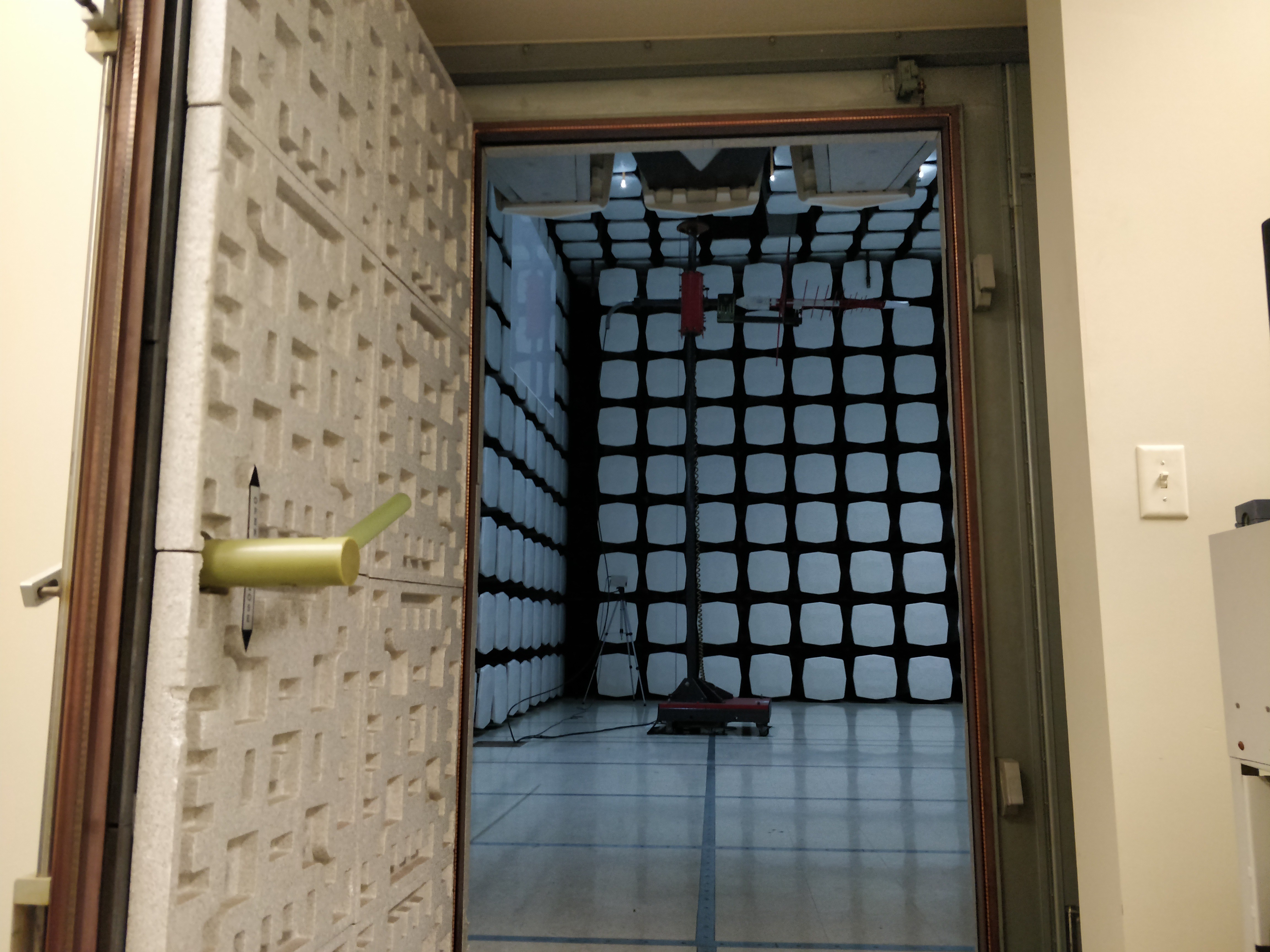
above, the 10m anechoic chamber entrance. Of note: the inner door handle is plastic. You can also see the low-frequency antenna mounted on its automated rising boom. This test is a farfield measurement, so the antenna is 10m from the target and measurements are taken with horizontal and vertical polarities from a variety of heights.
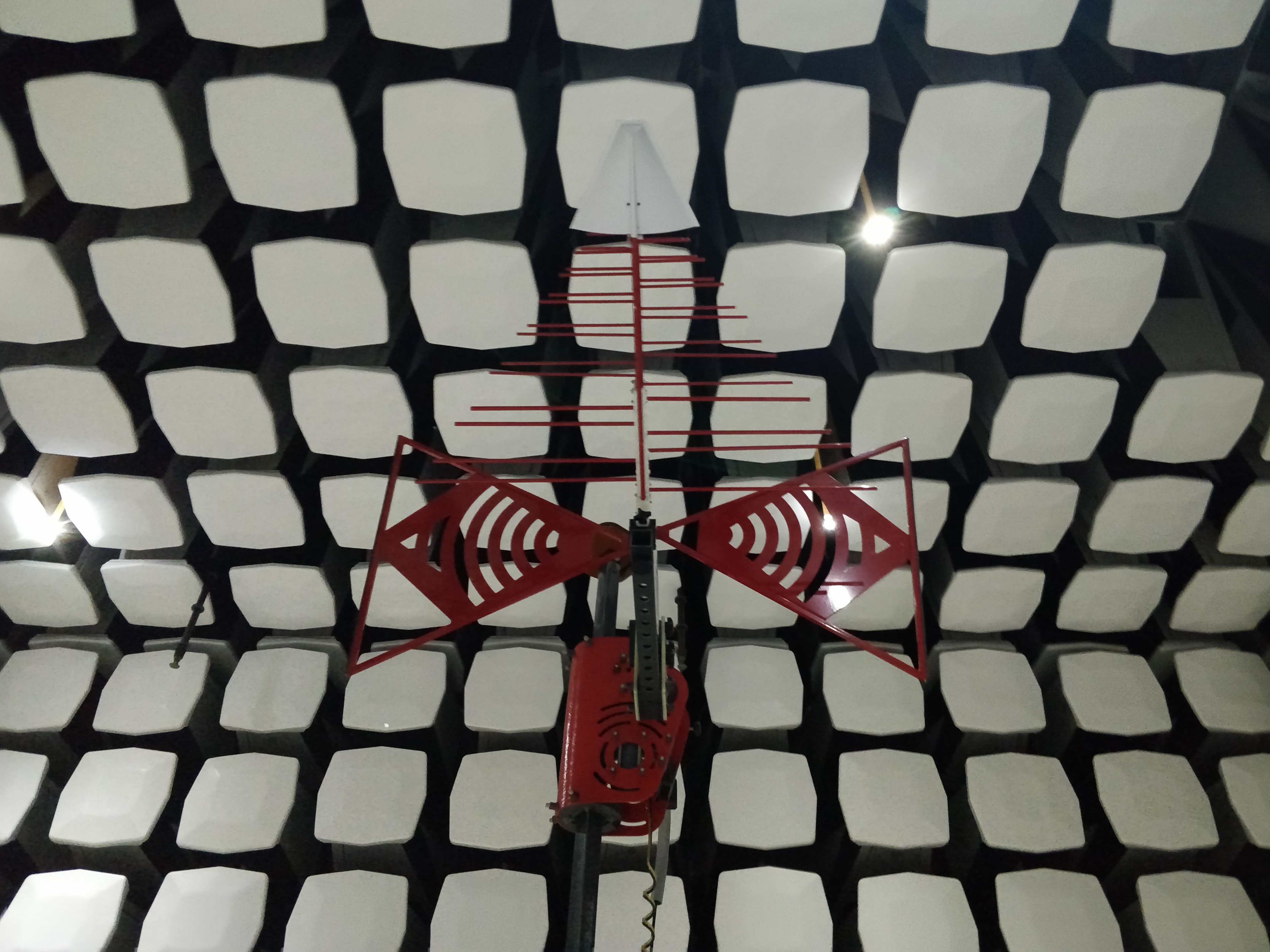
above, a close-up of the low-frequency antenna. Note the bizarre conductive foam anechoic panels (they are probably 600mm square and extend back into the wall 1m), and the expensive fiber-optic lights.

above, obligatory high-frequency antenna selfie. We didn't use this one since our equipment didn't have any active radiators (so we swept up to 1 GHz).
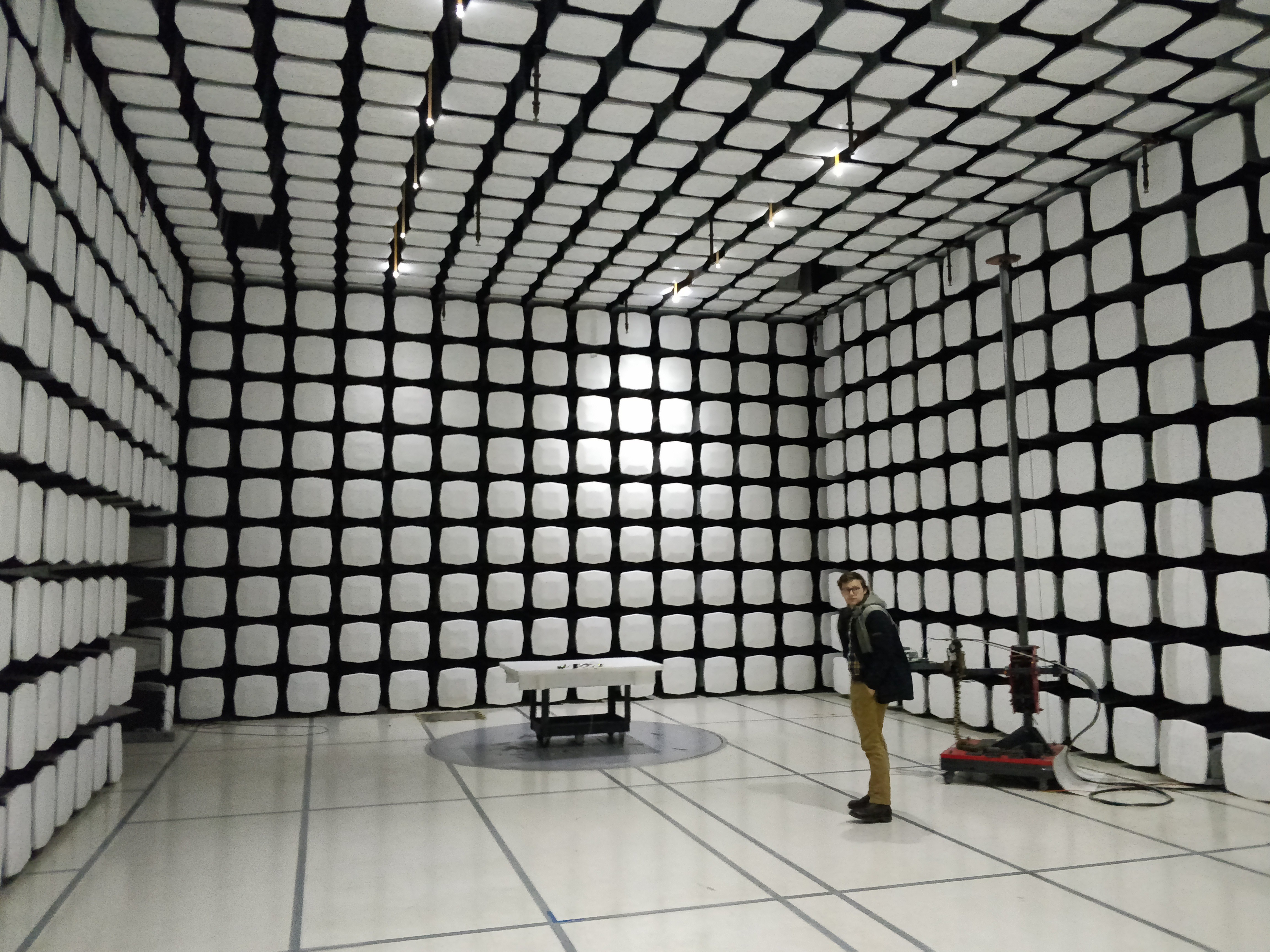
above, Jarod stands by the high frequency antenna. The table on the round floor piece holds the NeuroBytes network (barely visible) and rotates continuously during testing. We stashed the NID's tablet in the floor so it (hopefully) wouldn't interfere with results.
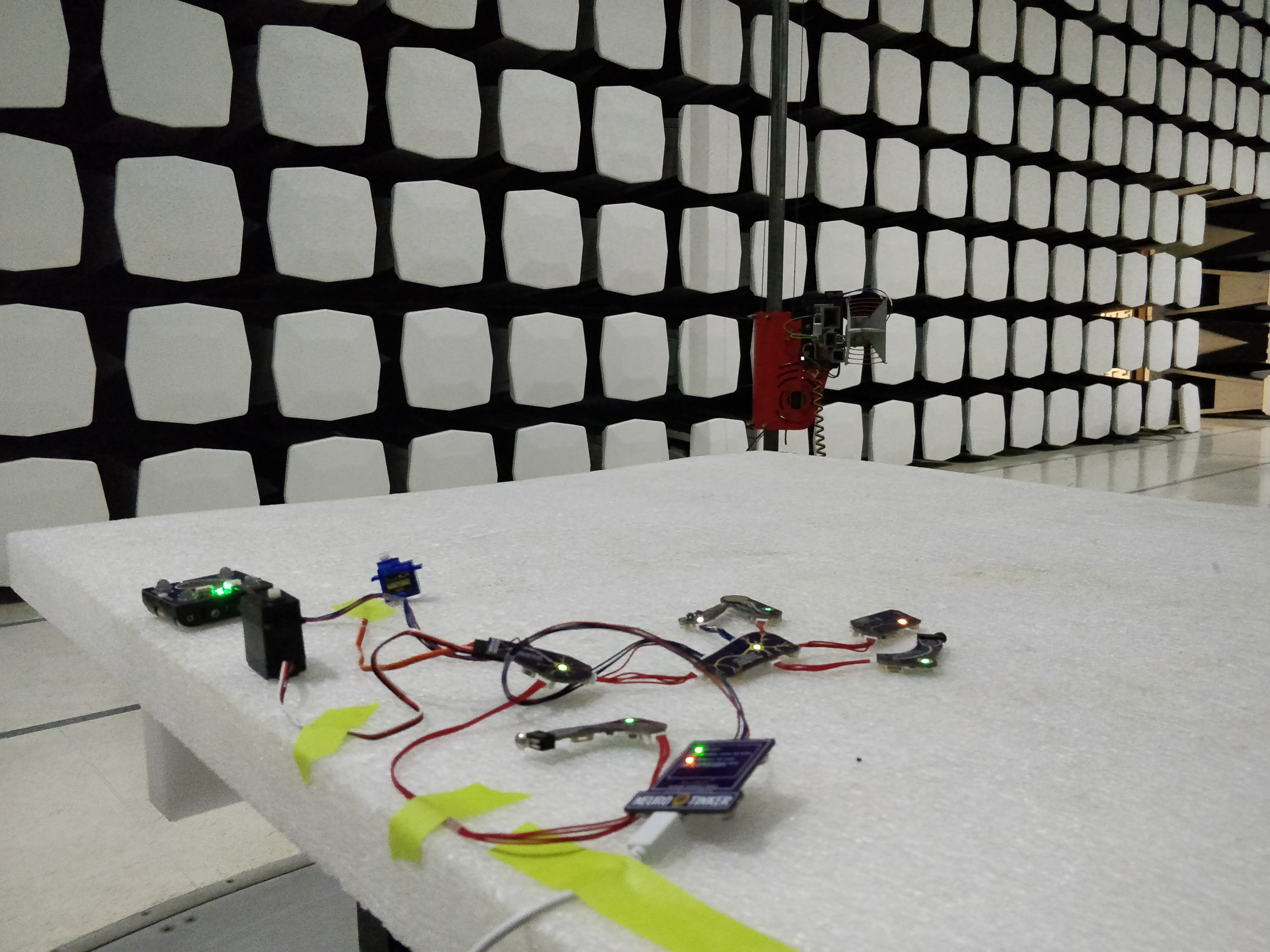
above, our chosen NeuroBytes network configuration for compliance testing. After consulting with the lab and a number of other sources we determined that a representative network with a 'typical' amount of traffic would suffice; testing boards individually would be cost prohibitive and, more importantly, not representative of how NeuroBytes are actually used.
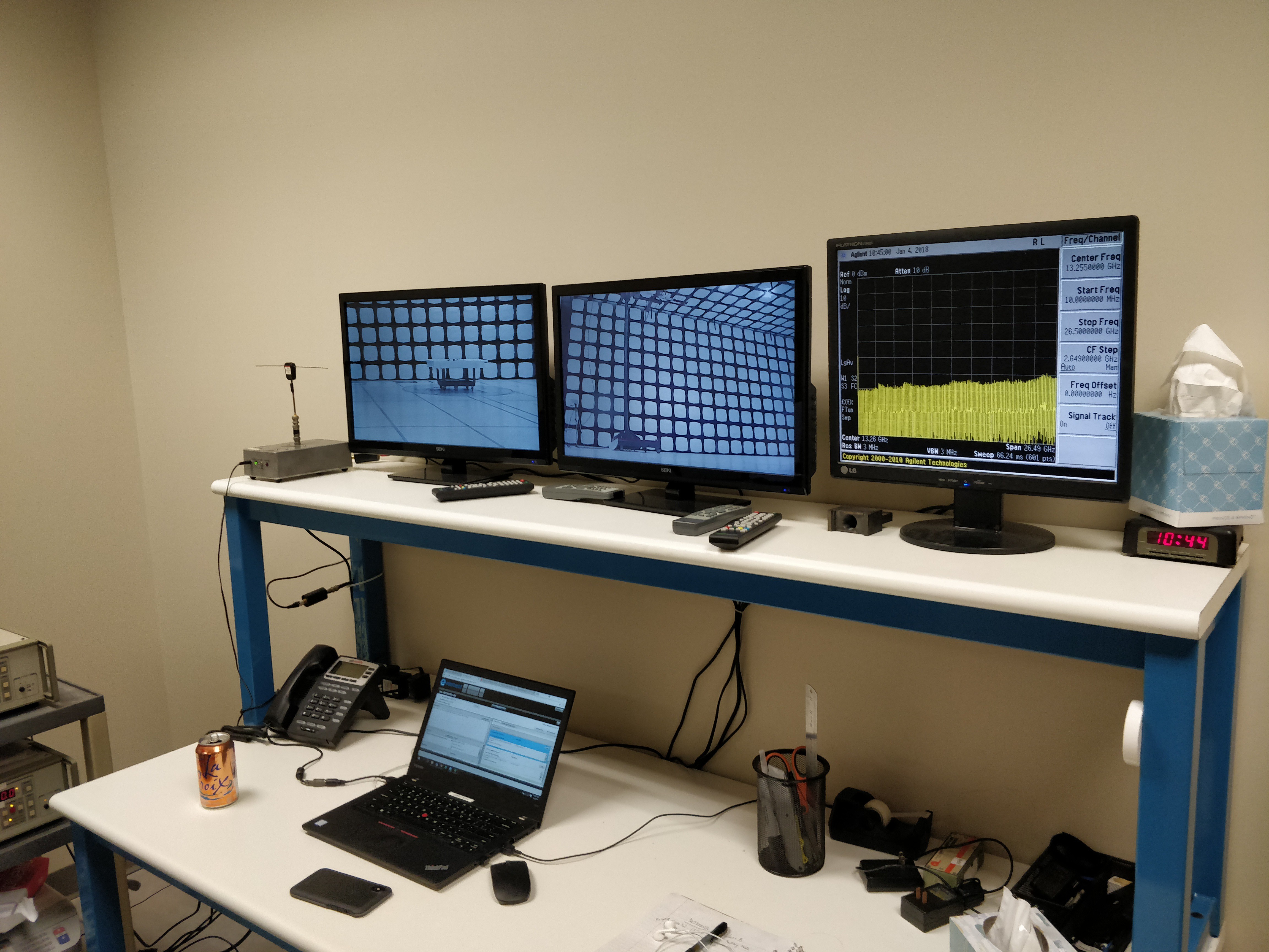
above, part of the analysis setup at the lab -- several shielded cameras recording the DUT (Device Under Test) along with a screen from their insanely fancy Agilent spectrum analyzer (whose model number I forgot to jot down).
Yeah, it was a neat experience, and the tech who worked with us for the 2-hour radiated emissions test was helpful and well-informed. Then we failed the test! Results:
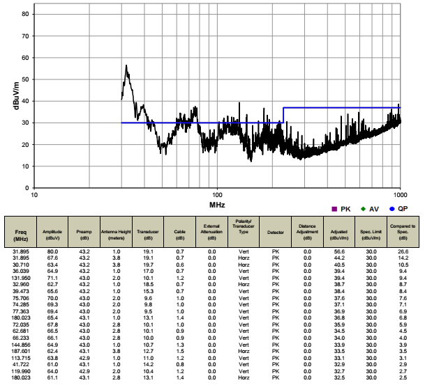 Above, a full NeuroBytes network test with the NID attached and the tablet graphing real-time data. This graph shows raw cumulative test data and we didn't actually fail in all the spots shown; after running through the quasi-peak detector we found that the first big hump (~30 MHz - 40 MHz) is the one we need to worry about.
We got the result above after a ~10 minute test, so we had plenty of time to try various experiments to narrow down the problem. I was concerned with rise time on the inter-neuron communication lines causing EMI spikes; our tech thought the USB cable may have been the issue. We didn't have any better-shielded or ferrite-equipped cables with us, so he tried snapping a giant 'suitcase ferrite' onto the USB cable:
 Above, maybe we're on the right track going after the USB cable? The 32 MHz peak is down quite a bit, but the 39 MHz peak jumped a few dBuV/m...
Not shown here, we also tried pulling both the continuous rotation servo and the micro-servo off the network; even though they're tiny I thought we might be seeing some commutation noise. No change.
Next, we ditched the tablet and USB cable entirely. Unfortunately this meant we didn't have data running between the NID and the first NeuroBytes board, but we wanted to be sure the emissions weren't coming from the inter-NB connections:
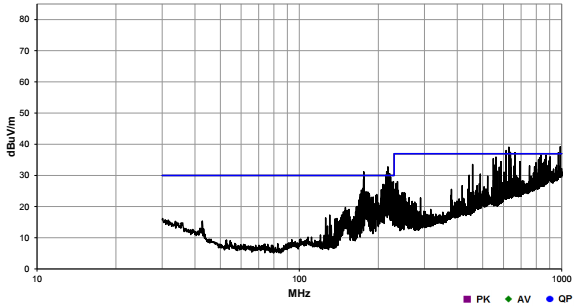 Above, bingo! The two peaks around ~110 MHz wouldn't cause a failure after quasi-peak detection so we're in the clear for a NB-only network.
Finally, as the end of the second hour approached, we ran a test with _just_ the tablet and NID. And we got some very strange results:
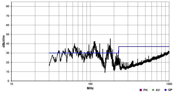 We didn't have time to do anything else, but I'm inclined to think that we were picking up excess EMI from the tablet itself; during testing it sat under the floor but the shielding had a fairly substantial (~150mm) hole, and the USB cable we brought was only 1m long.
 This wasn't our best day, but I think we learned a lot. For starters, we verified that NeuroBytes on their own are good to go with respect to EMI -- all the issues we encountered had to do with the USB communications between the NID and the tablet (with the aforementioned caveat regarding NID-->NeuroBytes comms not being independently tested). When we initially planned for EMI testing we considered doing some pre-tests, either in-house or at a lab, but decided to take a chance that we could pass based on extensive research and discussions with numerous more experienced engineers. It's probably a risk I would take again; re-creating EMI testing conditions in the lab is difficult and expensive, and pre-testing certainly doesn't come cheap either.
Having said that, our plan going forward has a few parts. First, we're going to recreate the results above in our lab, using a spectrum analyzer, a small test chamber, and a handful of hand-held nearfield probes. While these tests won't give us absolute data, we do have a few relative measurements (i.e. with USB and without) to compare to, so we should be able to see if any fixes we implement get us in the right ballpark.
Second, I bought a bunch of USB cables. Some are nicely shielded. Some have ferrites. All are longer than 1m, so when we go back for testing we'll be able to make sure the tablet is deep in the shielded floor area.
Third, we're going to play around with a few design elements -- improving ground planes where possible, adding ferrites and filter caps where needed, etc.
Fourth, we're going to do everything we can from a firmware perspective to increase rise times and eliminate high-frequency elements on the boards. Unfortunately we don't have a great deal of flexibility on the USB side (as it needs to be full-speed 12 Mbps for reasons I'll cover later), but we do have options.
And fifth -- I'd love to hear some ideas from you, dearest reader. Especially if you've been through radiated emissions testing and have thoughts about DIY testing. While we had the budget to re-test once, I have no intention of re-testing twice -- that means when we schedule our next visit to the lab, it should be the last.
 zakqwy
Discussions
Become a Hackaday.io Member
Create an account to leave a comment. Already have an account? Log In.
Condolences about the grade, but this is a really great log, and I appreciate this perspective.
The idea of running a kickstarter and not passing EMC scares the hell out of me
Are you sure? yes | no