 zakqwy
I started this project by measuring my wedding ring. I like its form factor and it fits well enough, and the wide curved stone on the top seemed like a nice element to replace with LEDs:
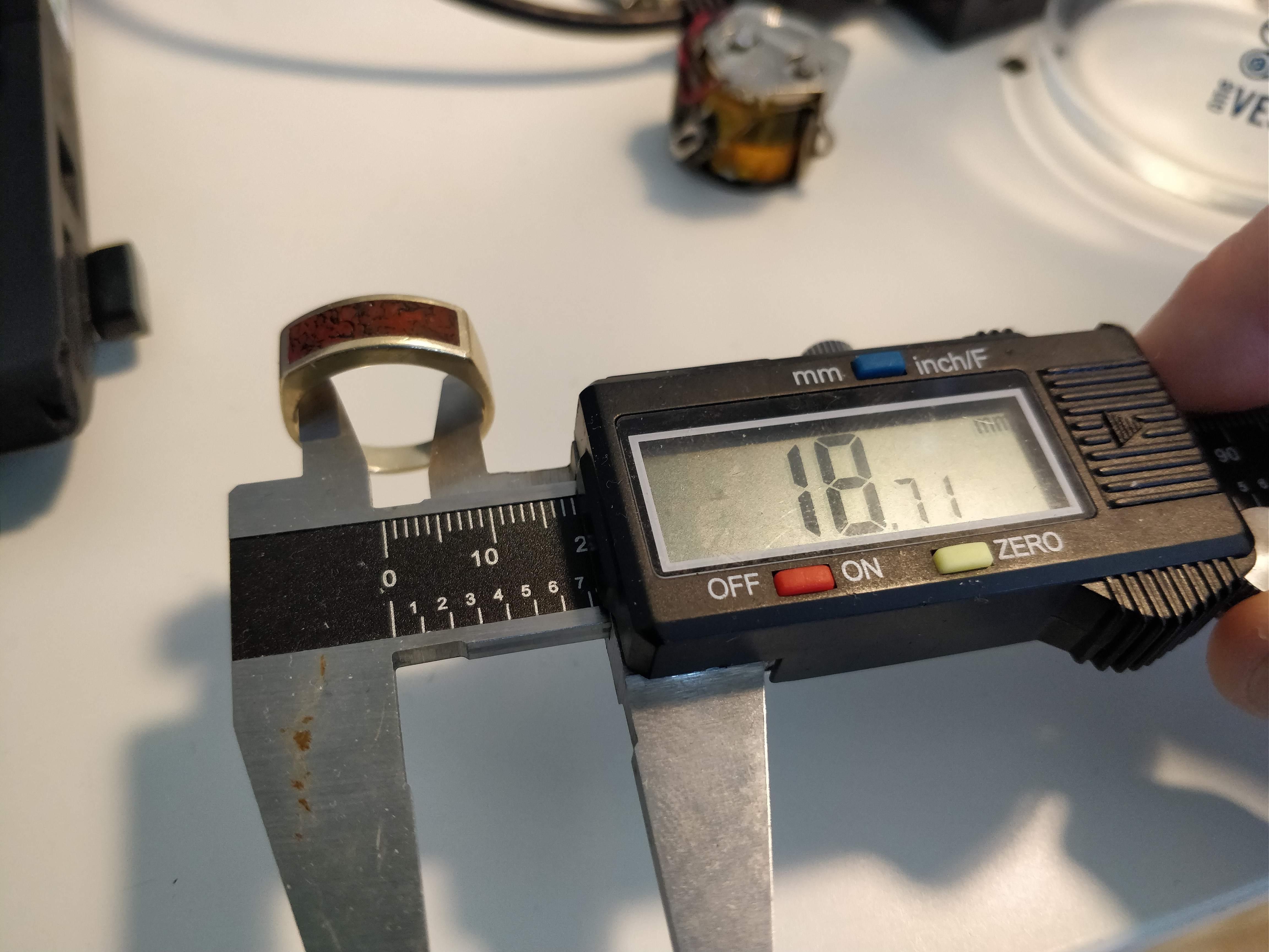
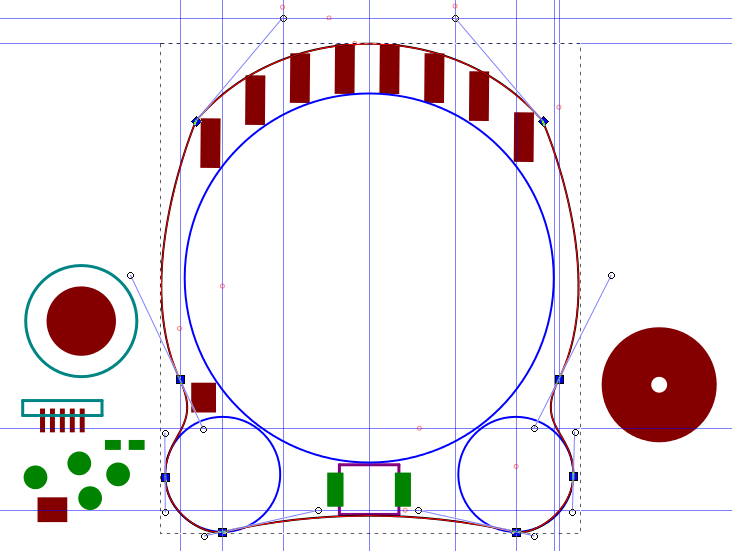
That got me in the ballpark; my fingers are all different sizes and I figured the PCB edge wouldn't be nearly as accommodating as a smooth gold band, so I decided on a ~19.5mm opening. After creating initial footprints in KiCad and pulling them into Inkscape (via *.svg export), I putzed about for a few hours and came up with a reasonable PCB outline:
 A few things to note here:
- I'm using Inkscape, not a nice parametric CAD program that allows dimensioning and complex constraints. As such, I depend heavily on guidelines and snapping to ensure dimensional consistency and (in this case) symmetry. Like all things, using this tool rather than something like Fusion360 or FreeCAD is a tradeoff.
- I tend to design organic shapes using the minimum number of points possible; in this case, the ring outline has 8 nodes, six of which are smooth. Again, I used guidelines to ensure node alignment and approximate handle positioning. But if you zoom in close enough, the ring isn't perfectly symmetrical.
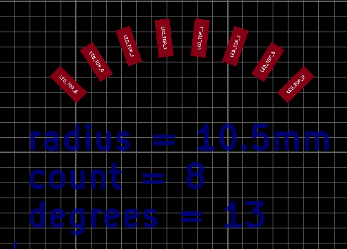
- I keep critical footprints in their own layer, and move them around as needed to get other dimensions correct. In this case, those footprints are mainly the batteries (the large red circles, one of which has a large hole for the Zn-air vent), the side-mounted pushbutton switch, and the LEDs. Note that the LEDs are linear-spacing-equalized but not rotated to final position; as fas as I can tell you can't do circular arrays in Inkscape, and in any case I wanted KiCad to identify them as discrete footprints rather than an imported graphic. The critical dimension here was width, so I used one footprint as a rough ruler and rotated it as needed to approximately equalize clearance between the inner and outer edge cut.
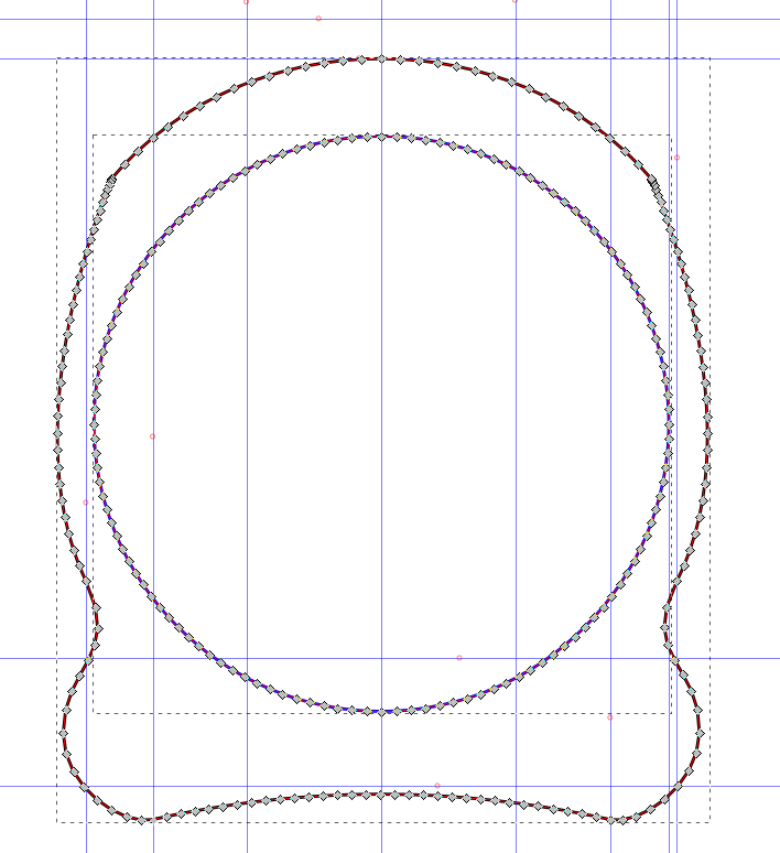
I then imported the outline as a *.dxf file (twice) into KiCad and got the two halves aligned on the same grid: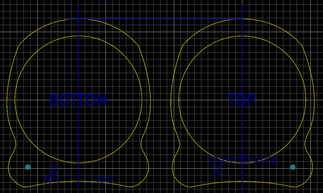
Note that I added the specs to the PCB comment layer, and manually named each LED footprint to its appropriate net. Then I deleted all the originally imported LED footprints. Probably a simpler way to do this, but it worked for me.
Routing was straightforward. I arranged the Charlieplexed LEDs in such a way that I minimized vias and was able to run the four signal lines as four pours around the skinny part of the ring, which avoided awkward jointed traces: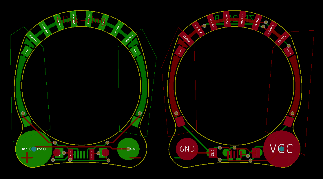
 Good enough. And yes, the ring does tend to pick up glove fuzz (seen on the LED), but so far it hasn't broken. Next... assembly notes!
Discussions
Become a Hackaday.io Member
Create an account to leave a comment. Already have an account? Log In.
Agreed! This stuff is super fun.
Inkscape protip, for future:
- Create square LED and circular path
- Select circle, Path->Object to Path
- Select square, then circle
- Extensions->Generate from path->Scatter
https://imgur.com/tysu8p5
Are you sure? yes | no
that is awesome! will remember that for future projects.. thanks!
Are you sure? yes | no
still awesome! keep doing weird stuff (and inspiring me to do more weird stuff)!
Are you sure? yes | no