 Hacker404
I started designing a PCB in CAD. I realised that it's not so easy to deal with these chips on a single sided board. The routing is a challenge.
After a little while I decided that instead I should start with something simple as I have never designed / made a PCB before.
I designed a tiny adaptor board to mount a SOJ36 chip on a standard width (0.6") DIP.
I chose the SOJ as that's about the hardest thing I am willing to try to solder. and I chose the 0.6" width to make is so cramped that trace widths and spacings are a challenge. I didn't expect it to work out but I did expect to find the limits.
The pins aren't in the correct order as there simply isn't enough room on a single sided board. That doesn't matter that much when it connects to CPLD as I can just fix the ordering inside the CPLD.
Here's the CAD -
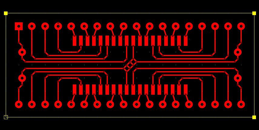
The traces are 10 mill and the spacing goes down to 15 mill.
Here is the toner and TRF transferred to the board -
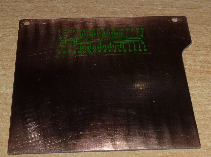
The TRF didn't bond propperly in some places. I am not sure why.
Here is the etched / drilled board -
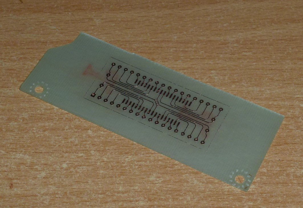
It has a few pits but I expected that for a first run. The fact that the TRF was missing in places didn't make any difference.
I tinned it with a big blob of solder then cleaned it off with solder wick -
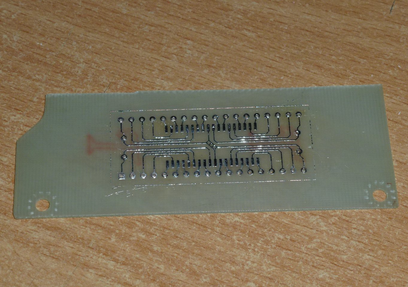
I soldered the chip on and then the header pins. I then tested for shorts and that everything connects as it should ... all good -
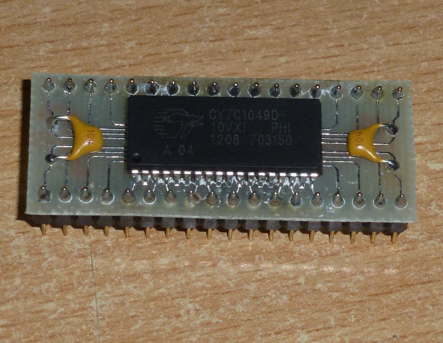
After taking this pic I realised how much flux is still under the chip. If I clean that out it may even work!
Discussions
Become a Hackaday.io Member
Create an account to leave a comment. Already have an account? Log In.