 twl
twlFeatures
- Supports 3/4 lane MIPI DSI displays.
- DSI controller supports resolutions of up to 1080x1920 at 60 Hz refresh rate.
- Converts HDMI video to DSI - letting you connect any MIPI DSI screen to your PC, Raspi or similar devices. Conversion works up to 720p@60 Hz or 1080p@48 Hz.
- Built-in framebuffer with simple graphics stack, allowing to interface small microcontrollers, such as Arduino through 8-bit parallel or SPI busses
- Sub-$50 BOM, including 4-layer PCB (@100pcs).
- Powered through mini USB connector.
- Embedded 32-bit CPU, available for user applications.
Project history
- 12/2013: Schematics & PCB done.
- 12/2013: Initial version of the firmware, works with Iphone4/4s screens on a FPGA dev kit.
- 02/2014: Got the PCBs and components.
- 02/2014: Test PCB assembled, drive both 3- and 4-lane screens.
- 07/2014: Started work on HDMI <> DSI conversion.
- 08/2014: HDMI convesion working for 640x960 Iphone4 screen.
- 08/2014: DSI core achieves 1080p @ 60 Hz (48 Hz with HDMI conversion).
- 08/2014: Rev 1.1. PCB design, schematics and firmware released.
- 06/2015: Prototypingr rev 2.0.
To do
- Arduino interface/drawing commands (depending on demand).
- Test external HDMI decoder with displays larger than 1080p.
- Port Doom to run on the softcore CPU.
Hardware
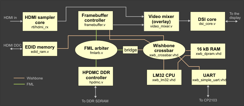
The diagram below shows the main blocks of the design:
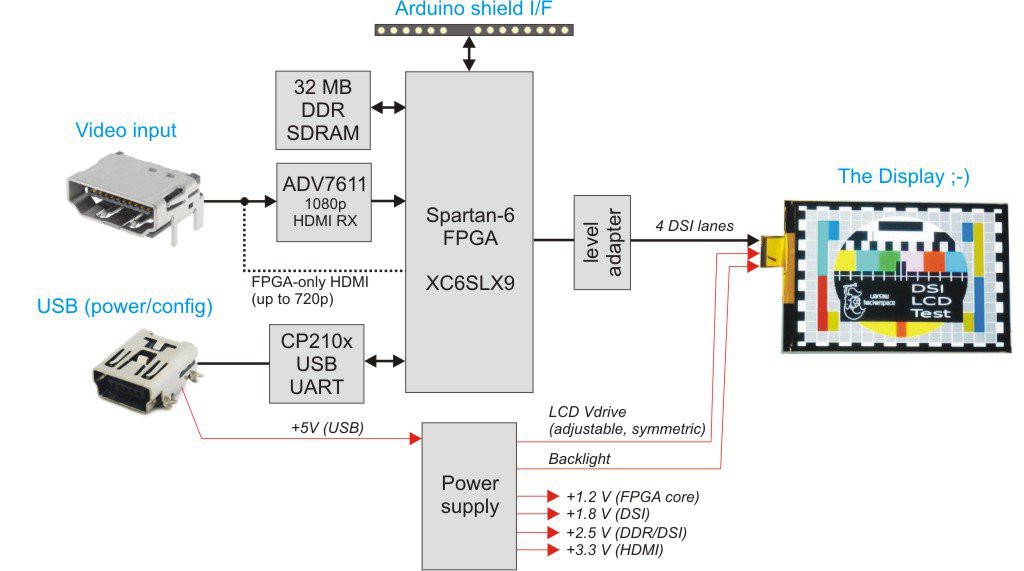
- The FPGA: Xilinx Spartan-6-SLX9. Highlights: amateur-friendly TQFP144 package and built-in SerDes rated up to 1080 Mbits/s. The FPGA does pretty much everything in this project, hosting the MIPI DSI core, framebuffer controller with DDR memory, HDMI/DVI decoder. Everything is managed by an embedded Lattice Mico32 CPU.
- DSI Level adapter: a bunch of resistors interfacing the FPGA's 1.8 V SSTL/LVCMOS I/O to DSI levels. More info in the FPGA section.
- DSI connector: a standard 2x15pin 2mm pitch female connector with all DSI signals, power supplies and some GPIO pins for interfacing with the display. Since connector pinouts differ between displays the idea here is to use a tiny adapter board hosting the particular LCD's connector and its wiring.
- DDR SDRAM, providing memory for the framebuffer, since most smartphone DSI displays don't have one.
- HDMI input: slow version, using FPGA's ISERDES blocks (up to 1080p @ 48 Hz) or a fast one (1080p @ 60 Hz), based on Analog Devices' ADV7611 chip. The external HDMI decoder shares some pins with the SDRAM chip and the host interface, so the full HD - 60 Hz version can only work as a HDMI to DSI adapter.
- Host interface: 12 pins wired to Arduino shield's IOH/IOL headers. Exact functions are not defined yet, I'm thinking about a 4-wire SPI interface and an 8-bit parallel bus.
- USB UART a CP2102 chip providing USB UART, software bootloader and JTAG functionality for the FPGA.
- Main power supply: integrated PMIC (TI/National LM26480). Voltages are: +3.3 V (HDMI input, USB, host I/F), +2.5 V (SDRAM and FPGA Vccaux), +1.8 V (DSI), +1.2 V (FPGA core).
- LCD bias/backlight power suply: Most displays need some higher positive/negative votlage to operate. The board has a simple DC/DC converter for that purpose, producing symmetric voltage of up to +/- 6 V. The voltage can be adjusted for the particular panel by connecting a resistor between one of the DSI connector pins and ground. There is also a separate current driver for backlight LEDs, programmable by another resistor. Both DC/DC converters use a TPS61041 chip.
PCB Design
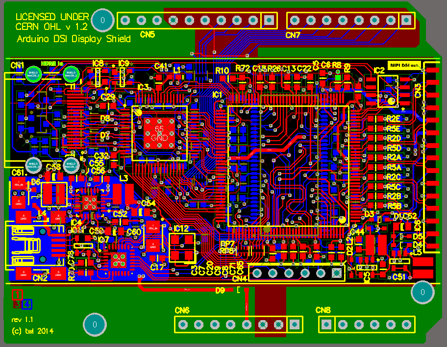
The DSI shield consists of two PCBs - the main board, where all the cool stuff is and a small adapter board, usually different for each display, connected through a 30 pin 2mm pinhead.
The main board is a typical Arduino shield. I routed the design on 4 layers, with the signals on the 2 outer layers, a contiguous ground plane and a split power plane. The DDR is placed right under the FPGA to simplify routing. SSTL to DSI level translator resistors are placed right next to the FPGA output pins to avoid stubs. All differential pairs are calculated for Z0=100 Ohm.
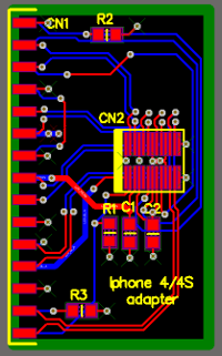
The adapter boards simply route the DSI lanes, power and backlight signals to the display's connector. There's completely no standard governing DSI LCD panel connectors and power, so for each display type you'll need a separate adapter board. They are meant to be simple (2 layers, a connector + few resisors for setting bias voltage/backlight LED current). The screenshot below shows the layout of the Iphone 4/4S Retina display adapter:
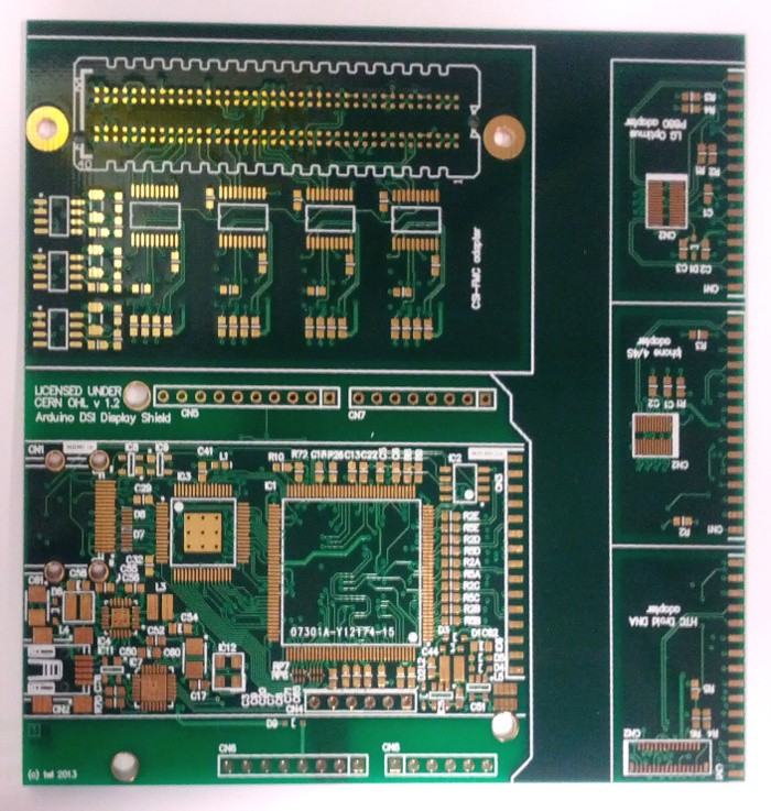
 The prototypes were made by Itead studio:
The FPGA
The heart and soul of the project: Xilinx Spartan-6 - low cost FPGA with gigabit SerDes blocks on each pin, which make it possible to sample HDMI/DVI signals or generate DSI data stream with just a bunch of external resistors. The intestines of the FPGA are shown below. For the moment it's just a very brief description of what's where in the Verilog/VHDL code.
CPU & Peripherals
The CPU is responsible for initialization of the display and controlling the framebuffer. It can also do some simple drawing operations (although not too fast).
I chose a Lattice Mico32 soft-processor due to maturity of the design and because other successful OSHW projects use it (e.g. Milkymist). The CPU controls the following peripherals through a Wishbone interconnect:
- A small 16 kB RAM block, containing the software. The first 2 kB are reserved for the bootloader, the remaining 14 kB is the actual application.
- An UART (for debugging and loading the software).
- The DDR memory (slow access through Wishbone to FML bridge).
- The Framebuffer and the DSI core (setting video mode timing).
- EDID RAM, pretending to be a 2402 I2C EEPROM. Tells the HDMI source of the timing requirements of our display.
DDR Memory & Framebuffer
The memory subsystem uses Milkymist's High Performance Dynamic Memory Controller (thanks Sebastien!), connected to a 32 MByte DDR RAM (16 bits, 100 MHz). The RAM is currently used to store only the displayed image, the CPU can't execute code from it. The framebuffer core simply pumps frame data from the DDR RAM to the video overlay engine, where it's composited with the HDMI video.
HDMI Sampler
HDMI/DVI decoder from Xilinx's application note XAPP495. Inputs HDMI, outputs parallel RGB pixels, clock and synchronization signals. Used pretty much as a black box here.
Video Overlay
Just as the name says, it puts together the images from HDMI and the framebuffer (using simple color keying) and outputs the final pixel stream for the display. Includes some elastic buffering and frame alignment logic between 3 different clock domains (HDMI clock, CPU system clock and the DSI core clock).
DSI Core
The architecture of the DSI core is shown in the diagram below:

The pixel pipeline consists of 5 stages:
- The first stage is a big 4096 entry FIFO. It's role is to move the RGB pixel data from the system clock domain to the DSI byte clock domain (= data rate divided by 8). Thanks to that, we don't need to keep the system running synchronously to the pixel clock - the pixels can come at a slightly faster/slower rate.
- The Timing generator produces a sequence of DSI High Speed (HS) packet headers and payloads, which indicate a horizontal/vertical synchronization pulse, blanking period or pass RGB data to the display. Display resolution and blanking timing is programmed by the CPU through Wishbone interface.
- The Packet assembler takes the packet requests, stuffs them on 3 or 4 parallel bytes, adding packet headers and footers with ECC/CRC checksums.
- The Lane control modules (4 for the data lanes, 1 for the clock lane) control the transitions between low power (LP) and high speed (HS) modes and generate LP mode signals to initialize and enable the display. At the output of the Lane control module, we get the LP+ / LP- signals and an 8-bit parallel data stream for the SerDes. The clock lane data output is simply fixed to 0xaa, resulting in a DDR clock at the output of the SerDes.
- The SerDes block - converts parallel 8-bit data to high speed serial bits using Spartan-6's OSERDES2 blocks. Also ensures correct timing between data and clock lanes, thanks to the IODELAY programmable delay lines at each FPGA pin.