Close
0%
0%

Nysa: FPGA Development Environment

Hardware and software to simplify FPGA development and interaction.

Similar projects worth following
FPGAs are awesome!

It's tough to get a project started though. If you want to design anything more substantial than blinking an LED, like interfacing with a camera, you need to spend a significant amount of time developing the infrastructure. Questions like, How to talk to the FPGA? can I use external memory? Will a new feature/core break the rest of the system?

This is what Nysa is for. It's a development environment that will glue your awesome, custom core to an internal bus inside the FPGA and it defines a communication scheme to communicate with you computer using a simple Python API.

The environment that generates an FPGA image from your cores also creates a small ROM that is inserted into the FPGA image. this ROM is read by the host (Desktop computer or MCU) and defines the behavior of the FPGA (What cores are in it) and their location within the FPGA.

This project was started over 3 years ago when I wanted to interface my Digilent Nexys 2 board with an LCD screen I saw on Sparkfun. it worked but it bothered me that starting an FPGA project was a huge undertaking. I wanted the process of adding a new device to be analogous to the Arduino ecosystem. Where trying out a new idea was as easy as downloading some code and adding small tweaks to make it fit into your design. I am so impressed with what artist and other hobbyists have done with a small MCU as the Arduino, I believe that if I could offer an FPGA development environment with similar capabilities then instead of projects consisting of LEDs and accelerometers we would see high functioning robots with vision pipelines.

Nysa was born (actually I called it Sycamore at first, then Olympus)

3 Years later Nysa can glue together an assortment of cores into an FPGA image graphically without writing one line of HDL.

Software:

The main repository is broken down into three parts.

  1. Core Builder (cbuilder): Scripts to help users generate custom cores. The tool generates verilog projects that contain not just the RTL but the build tools to verify (with iverilog) simulate and view waveforms (with gtkwave). When the user is satisfied they can use ibuilder to add their core to an FPGA image.
  2. Image Builder (ibuilder): Scripts to construct a custom FPGA image using the user defined core created with cbuilder and platform information to allow the host device to talk to the core. The build tool also uses the structure of the generated image to construct a ROM within the FPGA that can be used with the Host API to determine the behavior of the FPGA.
  3. Host: An API used to talk to the FPGA platform with an image created by ibuilder. The simple API consists of 'read' 'write' along with some helper functions.

Hardware:

There are two existing platforms I've been using Nysa with:

  • Dionysus: a small (low cost) Spartan 6 based devboard that is in the form factor of an Arduino and can communicate with the host computer using FTDI FT2232H USB 2.0 which allows the user to both download a new FPGA image and communicate with the it at a rate of about 25MB/s. It is much faster than other UART based interfaces and streaming low resolution video to and from it is possible play video
  • Prometheus: A higher end board using an Artix 7 FPGA with the intention that it will be used in high speed data acquisition, High definition video processing and SDR.

A board in the works is Artemis, first prototypes are starting fabrication in a couple of days. This is a board that has both high speed SERDES and DDR3 that will open up high video processing, SDR and, in general, more complicated projects. The board comes with two high speed connectors with the intention that the host interface can be changed from USB 2.0 to something like PCIE.

Nysa can be used with any available arbitrary FPGA devboards that supports external communication.

  • SATA, DDR3, Verilog Visualizer and Other Stuff

    Dave08/02/2015 at 23:24 1 comment

    SATA Status

    After weeks of painful debugging. I have been able to read and write to the hard drive!

    I ran into an issue though... the speed at which I can communicate with my FPGA to/from my computer maxes out at about 16MBs and the hard drive reads/writes data at a rate of about 250MBs. There was no way I could stress test the system reading and writing data directly to the hard drive from my host computer!

    I needed to verify that the SATA core can absorb and spit out an arbitrary large amount of data without errors...

    I started out by creating a temporary pattern generator and validator within the SATA core to write a pattern to the hard drives. Turn around and read that pattern back, verifying that the written data is read back correctly. Some debugging cycles later everything worked!

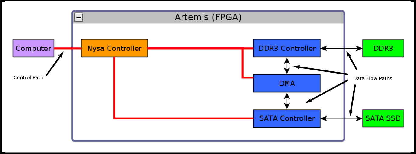
    But the end goal is to create a fast and useful way for users to store/load a large amount data generated or absorbed by their custom cores. It took a while to figure out how to create a test that exemplifies this but I think I got it. I combined the SATA, DDR3 and DMA cores for a test image. The host computer writes a 128MB test pattern (at a snails pace) into the DDR3. The DMA transfer data from the DDR3 to the hard drive and vice versa then the host can read the data out and compare it.

    Here is a block diagram of the test

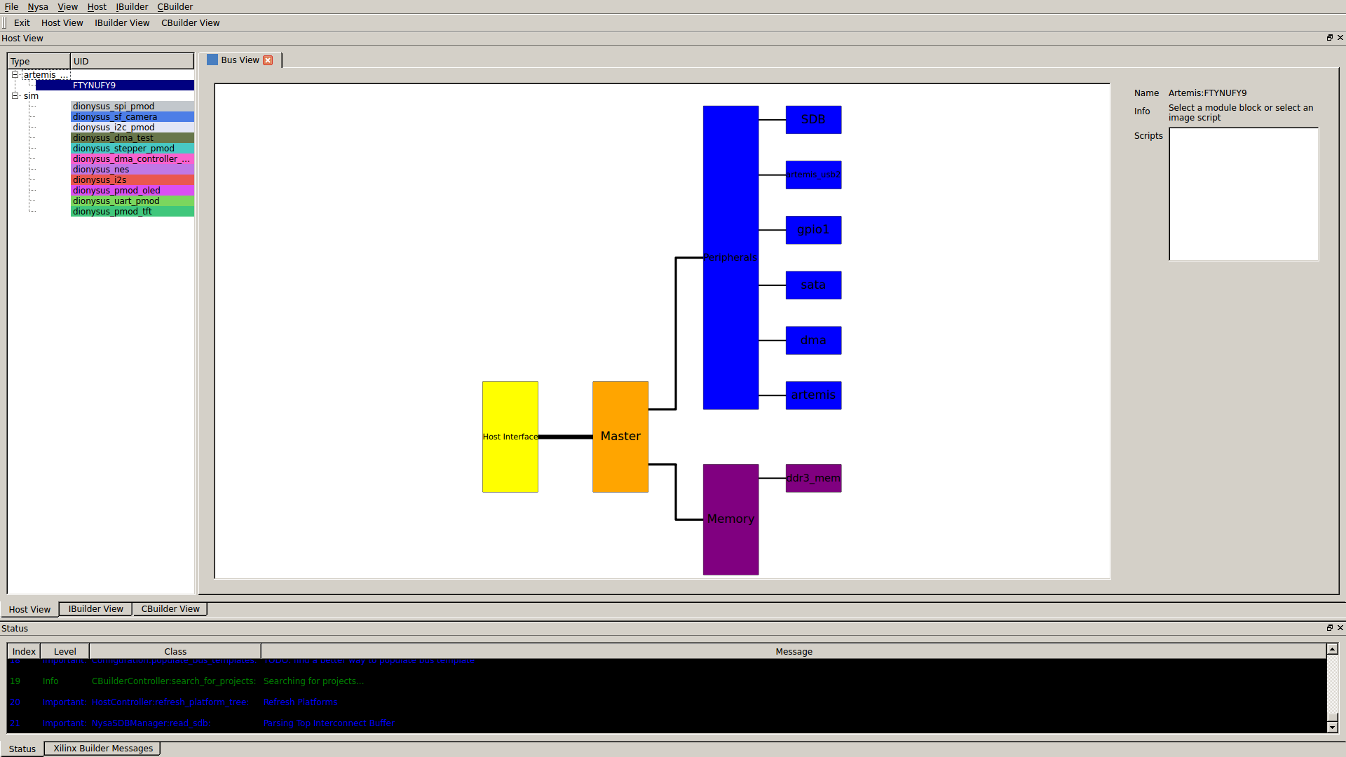
    I generated the Nysa image. Here is how the Nysa GUI looks:

    SO COOL! I've never had so many slaves on a Nysa image before! Each one of the blue modules above can control an actual core within the FPGA from the host computer. Users can interact with them through a simple Python interface.

    Now that I had control of the DDR3 memory, DMA controller and SATA hard drive I devised a test that validates the system, here is what the script does:

    1. Clear the hard drive, the host fills the DDR3 with zeros and writes that data to the SATA hard drive.
    2. Write a test pattern, the host fills the DDR3 with a test pattern, then the DMA writes this pattern into the hard drive.
    3. Clear the DDR3, the host fills the DDR3 with zeros so any data read from hard drive can not be mistaken for old memory data.
    4. Read the contents of the hard drive into DDR3 memory.
    5. Read all the values out of the memory and verify that the values correspond to the original test pattern.

    I understand the following is a little cryptic but this is the output. If something went wrong there would have been a lot of unfriendly messages telling me that numbers do not match, or worse the hard drive just hangs:

    cospan@loki ~/Projects/nysa/test/hardware $ (master) ./test_dma_sata.py 
    Important: Test:setUp: Found a nysa instance: FTYNUFY9
    Important: NysaSDBManager:read_sdb: Parsing Top Interconnect Buffer
    Info: Test:setUp: Using Platform: artemis_usb2
    Info: Test:setUp: Instantiated a SATA Device: /top/peripheral/sata
    Info: Test:setUp: Instantiated a DMA Device: /top/peripheral/dma
    Info: Test:test_dma_sata: Reseting Hard Drive...
    Info: Test:test_dma_sata: Reset Complete
    Important: Test:test_dma_sata: Linked up with Hard Drive!
    Info: Test:test_dma_sata: 	Initial Status of hard drive (Status): 0x50
    Verbose: Test:test_dma_sata: Hard Drive Serial Number: 132481400420        
    Verbose: Test:test_dma_sata: Max User Sectors: 33570816
    Verbose: Test:test_dma_sata: Max User Size (GB): 17.188258
    	SATA Status:                       0x00000050
    	SATA Sector Count:                 0x00000001
    	SATA Current Address:              0x00000000
    Info: Test:test_dma_sata: Setup DMA
    Info: Test:test_dma_sata: Transfer Size: 0x00A00000
    Verbose: Test:clear_memory: Clearing Memory
    Verbose: Test:clear_memory: Memory Size: 0x00000000
    Verbose: Test:clear_memory: Memory Size: 0x08000000 is larger than read/write size
    Verbose: Test:clear_memory: 	Breaking transaction into 0x00800000 chunks
    Verbose: Test:clear_memory: Cleared: 0x00000000 - 0x00800000
    Verbose: Test:clear_memory: Cleared: 0x00800000 - 0x01000000
    Verbose: Test:clear_memory: Cleared: 0x01000000 - 0x01800000
    Verbose: Test:clear_memory: Cleared: 0x01800000 - 0x02000000
    Verbose: Test:clear_memory: Cleared: 0x02000000 - 0x02800000
    Verbose:...
    Read more »

  • FPGA Timing Post

    Dave06/10/2015 at 15:55 0 comments

    I removed the previous post because I found there is better ways to solve the problem and I didn't want to lead anyone in the wrong direction (including my future self).

    When I have a better understanding of the subject I'll re-post the entry.

    Dave

  • SDB (Self Describing Bus)

    Dave05/31/2015 at 15:06 1 comment

    I started working on Nysa over three years ago. At the time I was working with a software guy who seemed to be allergic to FPGAs, he said that all of his experiences with them has been tedious, frustrating and required long conversations with the guy writing the FPGA code.

    The problem was this: When you want to talk to an FPGA using some controller the controller and FPGA need to be designed in concert. If the designer adds GPIOs to the FPGA the controller needs to know about the GPIOs including their location and characteristics. How to solve this?

    One method would be to document all the behaviors of the FPGA design and then use this document to design the software. This is obviously prone to errors, any late night changes to the FPGA code (HDL) and missed documentation would result in a communication break down. Another approach is to use something like USB Descriptors. If you are curious and you have a Linux box you can look at all the USB devices attached to your computer using:

    cospan@yogurt:~$ lsusb
    Bus 001 Device 003: ID 0483:91d1 STMicroelectronics 
    Bus 001 Device 002: ID 8087:8000 Intel Corp. 
    Bus 001 Device 001: ID 1d6b:0002 Linux Foundation 2.0 root hub
    Bus 003 Device 001: ID 1d6b:0003 Linux Foundation 3.0 root hub
    Bus 002 Device 004: ID 0bda:5720 Realtek Semiconductor Corp. 
    Bus 002 Device 003: ID 04f3:0296 Elan Microelectronics Corp. 
    Bus 002 Device 002: ID 8087:07dc Intel Corp. 
    Bus 002 Device 001: ID 1d6b:0002 Linux Foundation 2.0 root hub
    

    Then for more details into some device you can type (looking at the first device):

    cospan@yogurt:~$ lsusb -d 0483:91d1 -v
    
    Bus 001 Device 003: ID 0483:91d1 STMicroelectronics 
    Couldn't open device, some information will be missing
    Device Descriptor:
      bLength                18
      bDescriptorType         1
      bcdUSB               2.00
      bDeviceClass            0 (Defined at Interface level)
      bDeviceSubClass         0 
      bDeviceProtocol         0 
      bMaxPacketSize0        64
      idVendor           0x0483 STMicroelectronics
      idProduct          0x91d1 
      bcdDevice            0.28
      iManufacturer           1 
      iProduct                2 
      iSerial                 3 
      bNumConfigurations      1
      Configuration Descriptor:
        bLength                 9
        bDescriptorType         2
        wTotalLength           34
        bNumInterfaces          1
        bConfigurationValue     1
        iConfiguration          0 
        bmAttributes         0xe0
          Self Powered
          Remote Wakeup
        MaxPower              100mA
        Interface Descriptor:
          bLength                 9
          bDescriptorType         4
          bInterfaceNumber        0
          bAlternateSetting       0
          bNumEndpoints           1
          bInterfaceClass         3 Human Interface Device
          bInterfaceSubClass      0 No Subclass
          bInterfaceProtocol      0 None
          iInterface              0 
            HID Device Descriptor:
              bLength                 9
              bDescriptorType        33
              bcdHID               1.10
              bCountryCode            0 Not supported
              bNumDescriptors         1
              bDescriptorType        34 Report
              wDescriptorLength    3177
             Report Descriptors: 
               ** UNAVAILABLE **
          Endpoint Descriptor:
            bLength                 7
            bDescriptorType         5
            bEndpointAddress     0x81  EP 1 IN
            bmAttributes            3
              Transfer Type            Interrupt
              Synch Type               None
              Usage Type               Data
            wMaxPacketSize     0x0040  1x 64 bytes
            bInterval               1
    

    Although it looks odd this gives all the information to the host computer to either use a built in driver like a mouse/keyboard controller or enough information to tell the user that it needs a custom driver, and who is the vendor that should provide that driver (STMicroelectronics in this case).

    This is awesome and it would be great if it was easy to design an FPGA image that generated a descriptor such as this. I tried that a couple of years ago. It worked... ish, well it worked but it was lacking a lot of functionality. I called it the DRT or the Device ROM Table. The idea was the user specified a configuration file that would be used to program the FPGA and the script that generated the FPGA image would also generate this DRT at a known location within the FPGA. The controller would then read the DRT and know enough information to talk to the device. Essentially the FPGA itself was all the documentation required for the software developer.

    The DRT worked out great for about a year and a half, it was limited in that it gave only the bare essentials of what was needed. I would add more features hesitantly knowing that I might one...

    Read more »

  • Artemis Status and Gigabit Transceiver

    Dave05/28/2015 at 19:34 0 comments

    Artemis is alive an well!

    Artemis is working really well, most days I leave it attached to a Linux server at my office and remotely play with it when I get a chance. Work keeps me really busy so I can't dedicate too much time during the day but at night it's a different story.

    Artemis uses a Spartan 6 LX45T instead of Dionysus's Spartan 6 LX9, the '45' and '9' in the name is a loose indication of the programming space available inside the FPGAs so Artemis gives me roughly 5X logic space. On top of that the DDR3 hardware and HDL has checked out and man is that DDR3 fast!

    DDR3

    Because the Xilinx coregen creates a DDR3 core that has multiple ports a system can be designed to use many individual memory interfaces instead of using an arbiter to arbitrate the memory resource (this is how Dionysus works). This got me thinking about employing the DDR3 memory in more applications. It sounds great but writing custom DDR3 controllers for each high throughput cores is a big deal. After thinking about it for a while I decided I should write a DMA controller that has a simple FIFO like interface this is trivial to implement in a custom core. This way instead of attaching cores directly to memory I can attach them to a DMA controller and let it route the data to/from the DDR3 as needed. The DDR3 is so fast it can absorb data at a higher rate than most of the peripherals can generate or absorb. So it makes sense to use it as a buffer.

    I finished a version of the DMA Controller. It ended up having 4 input ports and 4 output ports, it can be configured using 8 instructions and it can bond channels, essentially behaving as a double buffer.

    DMA Controller FLow

    SATA

    I wrote a SATA hard drive controller a few years ago and I verified its functionality with a Virtex 6 FPGA. I posted the core on opencores nysa-sata. It works but it's difficult to use. I want to get the SATA controller to work on Artemis. I have a plan, it involves setting up the gigabit transceivers, configuring them to work with SATA and attaching the controller.

    I've already started on this plan and it is progressing well:

    Currently the GTP Transcievers seem to be alive. I wrote a small application that shows the transceivers are out of reset and the internal PLLs have locked on to the 150MHz SATA reference clocks and 100MHz PCIE reference clock. I am bringing the SATA core out of mothballs and adapting it to the wishbone bus. Last night I just finished the bare minimum port to wishbone so that I can make sure I can link up with the hard drive. Once this is finished I'll work on adapting the data interface to talk to the DMA controller.

    Hardware Respin Required

    Unfortunately, I found that a hardware respin is required of both Artemis and the host adapter board primarily because of connectors and I forgot to route a reset signal from the host control board to the main Artemis board. The new connectors will be more robust and the reset signal is trivial. Before I pull the trigger on an expensive fabrication and assembly I want to finish up the SATA checkout on this board. This will assure that I didn't make any mistakes while laying out the gigabit transceiver signals.

    I'll post some pictures soon.

  • Artemis

    Dave04/08/2015 at 15:12 0 comments

    Artemis!

    Artemis attached to the USB 2.0 and PCI Express Board
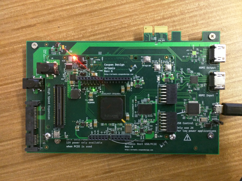

    FAB to Assembly

    Artemis came from fab about two months ago. I had hoped I could assemble the entire board myself in order to save some money. The FPGA and DDR3 came pre-balled with ROHS (lead free) solder so I didn't need to put down any solder paste. So I put the FPGA and memory chip on the board and ran it through the reflow oven. It looked like it worked until I bumped the board and both chips fell off.

    After a couple more attempts I asked my friend at MIT Media Lab to let me use the BGA rework station. We spent half a day there putting on FPGAs and memory chip. It looked like it worked so I went to ahead assembling the rest of the board. It was about 1 AM and I was nearly finished when I looked down at the board and noticed the DDR3 had slid sideways... the DDR3 didn't stick then either. I tentatively tested the FPGA and it was only attached by a couple of balls... GRRR!

    I decided to bite the bullet and spend about $1,000 to get the boards assembled.


    Smoke to Nysa

    Finally it was time for the smoke test. Success! Artemis held onto it's smoke. All regulators were outputting the correct voltages. I moved on to testing the FPGA. I created a simple LED blink app to test out the FPGA, LEDs, buttons and 100MHz oscillator. Success! I attached the new host interface board and after about a week of modifying a controller I used to interface with Dionysus I was able to download my first Nysa image. It was about that time I realized that I made a mistake in the design of Artemis... NO RESET BUTTON! ARGGH! I had to add an external wire but the correct solution is to add a open drain reset signal will pull the pre-existing reset pin on the Artemis base low from the host computer. This is useful so that I don't have to physically reset the board all the time.

    DDR3

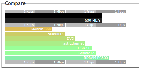
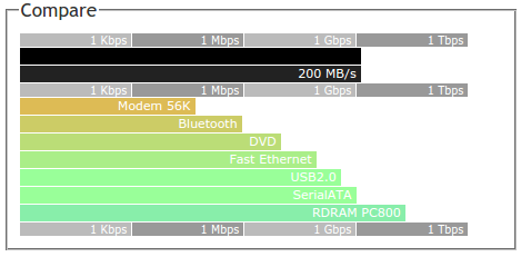
    Dionysus, the small board I used to test out Nysa, had a 16-bit 100MHz SDRAM chip as the memory source. To get an idea of what is possible with SDRAM I generated the following comparison charge using this great website: Forret Tools


    The DDR3 is obviously faster, it has an 8-bit interface at a double data rate running at 300MHz, so it equates to 1 byte @ 600MHz or this new comparison:


    I used the built in DDR3 memory core generator from Xilinx Coregen to create and interface with the memory, then wrote a wishbone wrapper around it and after about a week I verified that I could write to all 128MB and read it back correctly!

    I did run into an issue that I wanted to mention. Xilnx Coregen generates Verilog source code that I am not legally allowed to distribute so I figured out a way to generate a NGC file that users can instantiate. Its the equivalent of distributing a binary version of a library.

    What next

    I realized that in order to take advantage of the DDR3 I needed to design a DMA controller that could pull data from something like a camera put it into DDR3 memory temporarily and then store it into the SATA hard drives or output it to HDMI. It has turned out to be a complicated core. Once this is finished I am planning to design a stereo CSI camera board to test it out.

  • Dionysus 0, Mario 1

    Dave01/01/2015 at 18:23 0 comments

    I finally hit the limit of the little Dionysus and it came in form of the Nintendo Entertainment System.

    Dionysus has 9K Luts. In the world of FPGAs that gets eaten pretty fast by the infrastructure of Nysa. Not to say you can't interface with LCDs, Cameras and Audio but when the design is more complicated like, say a NES, the MAP tool will barf

    Slice Logic Utilization:
      Number of Slice Registers:                 6,491 out of  11,440   56%
        Number used as Flip Flops:               6,474
        Number used as Latches:                     11
        Number used as Latch-thrus:                  0
        Number used as AND/OR logics:                6
      Number of Slice LUTs:                     10,074 out of   5,720  176% (OVERMAPPED)
        Number used as logic:                   10,028 out of   5,720  175% (OVERMAPPED)
          Number using O6 output only:           8,008
          Number using O5 output only:             562
          Number using O5 and O6:                1,458

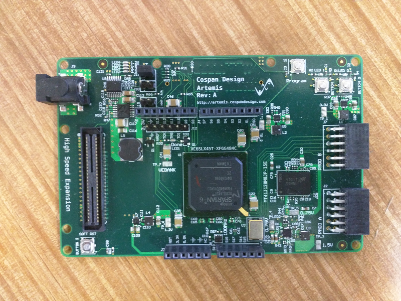
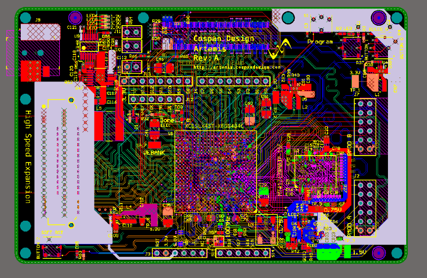
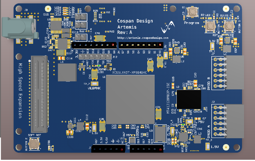
    This has prompted me to move forward with Artemis. A devboard with a larger FPGA, DDR3 and a flexible interface for both communicating with the board and expanding its capabilities. Here is the current view of Artemis:

    Along with all the connectors of Dionysus there is a high speed expansion that contains 50 Single ended, 25 Differential connectors as well as two SERDES Channel each capable of rates at about 3Gbps. I spent a long time debating whether to use this non-standard connector as opposed to the standard FMC connector but I have two reasons:

    1. The FMC Connector is $17.50 each!
    2. Hobbyist cannot make expansion boards without paying the prohibitively high prices for assembly. In order to get the FMC mating connector on an expansion board developers will need to pay for either assembly or some clever homebrew trick. With this you can possibly solder it by hand or use a heat gun to mount this. I hope this will help developers with less money to make some great projects.

    I'm looking forward to implementing image pipelines and SDR based projects.

View all 6 project logs

Enjoy this project?

Share

Discussions

Similar Projects

Does this project spark your interest?

Become a member to follow this project and never miss any updates