 Christoph
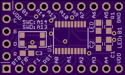
After I figured out the flaws in the current layout it was fairly easy to take care of them. The new layout has exactly the same size and pinout as the old one, but
- moved silk screen labels further away from SWD header,
- smaller silk screen text for more labels and hints,
- no more silk screen above vias,
- added reset cap,
- moved LED, resistor, and decoupling caps further away from each other for easier assembly (other parts got pushed around while placing them with my tweezers),
- changed LED current limiting resistor to 330 ohm,
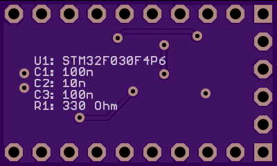
- updated bottom silk screen,
- added labels for the connections SWDCLK - PA14, SWDIO - PA13, and LED - PB1.
Preview:
Discussions
Become a Hackaday.io Member
Create an account to leave a comment. Already have an account? Log In.
I like this "print the values on the backside" approach!
Are you sure? yes | no
Thanks - I do this to avoid that feeling of cluelessness when I see an
old unused PCB and have no idea what it might be for. Happens too
often...
Are you sure? yes | no