 Jackson Keating
Powered through the pour and the via stitching. Never thought about how the number of traces inherent to a breakout board might impact the grounding plane that I need.
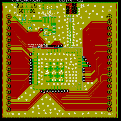
I don't know much about RF. For the sake of speed, I'm trying to rely on the reference designs from TI. Based on the reference design, I tried to maintain a solid ground plane throughout the top layer. At first, I had all of the breakout traces routed on the top layer. This prevented the majority of the board from being filled in by the copper pour. I made the call and moved all of the breakout traces to the bottom layer. This will provide a continuous ground plane for the top layer. Which again. I'm not sure is important at all.
Stitching with KiCAD is very counterintuitive. Luckily I found this handy video from Contextual Electronics:
And! It was the first hit in the google search. Made the whole process mostly painless.
Here's a snapshot of the first draft of the PCB. Barring anything that I remember when I'm less sleep deprived, it should be ready to upload to OSH Park. I'll give myself time to review it tomorrow and hopefully get it out.
Then it's back to firmware in order to write the programmer code.
Discussions
Become a Hackaday.io Member
Create an account to leave a comment. Already have an account? Log In.