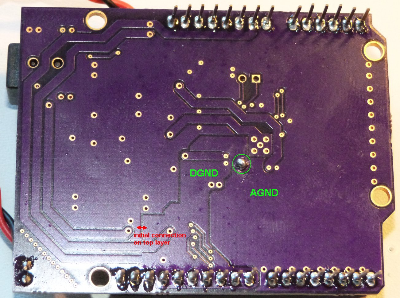
Next step in the test process was to loop back a DAC value into an ADC and compare the result to the output value. The read back ADC value was in the order of 24 LSBs lower than the original output value. For example at a voltage range 0-10V a DAC value of 0x400 resulted into a output voltage of 2.4920V but the ADC value was always around 0x3e8.
Tests with an external voltage reference and a linear regulator instead of the switched capacitor voltage converter for the negative rail did not show any improvement.
The issue revealed itself while monitoring the analog voltage rails and SPI communication was active. During every SPI data transfer, a lot of noise was visible on the analog side. This pointed to a less than optimal GND connection point between analog and digital GND. Tying the 2 GNDs together direct under the analog IC instead of the original place close to the optional digital regulator, solved the issue.

Now the loopback test shows a variation of 2-3 LSBs, which is a very good improvement.
 MagicWolfi
Discussions
Become a Hackaday.io Member
Create an account to leave a comment. Already have an account? Log In.