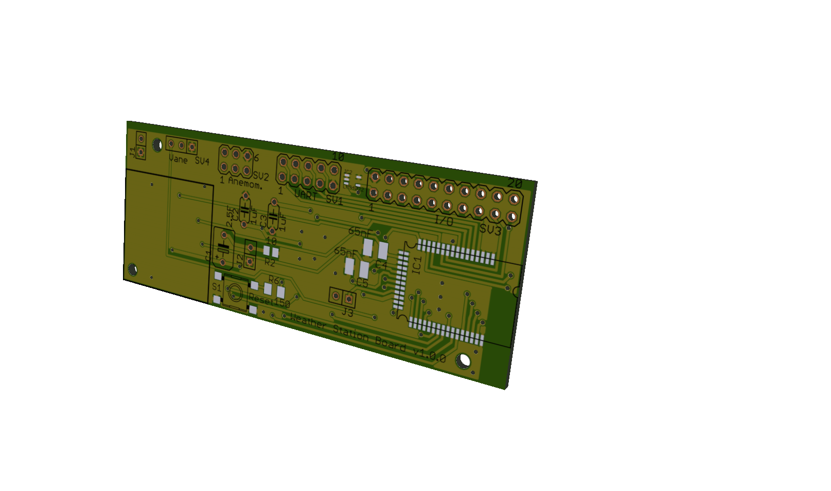
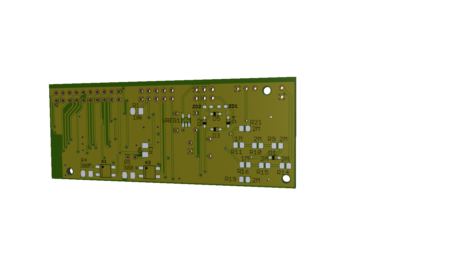
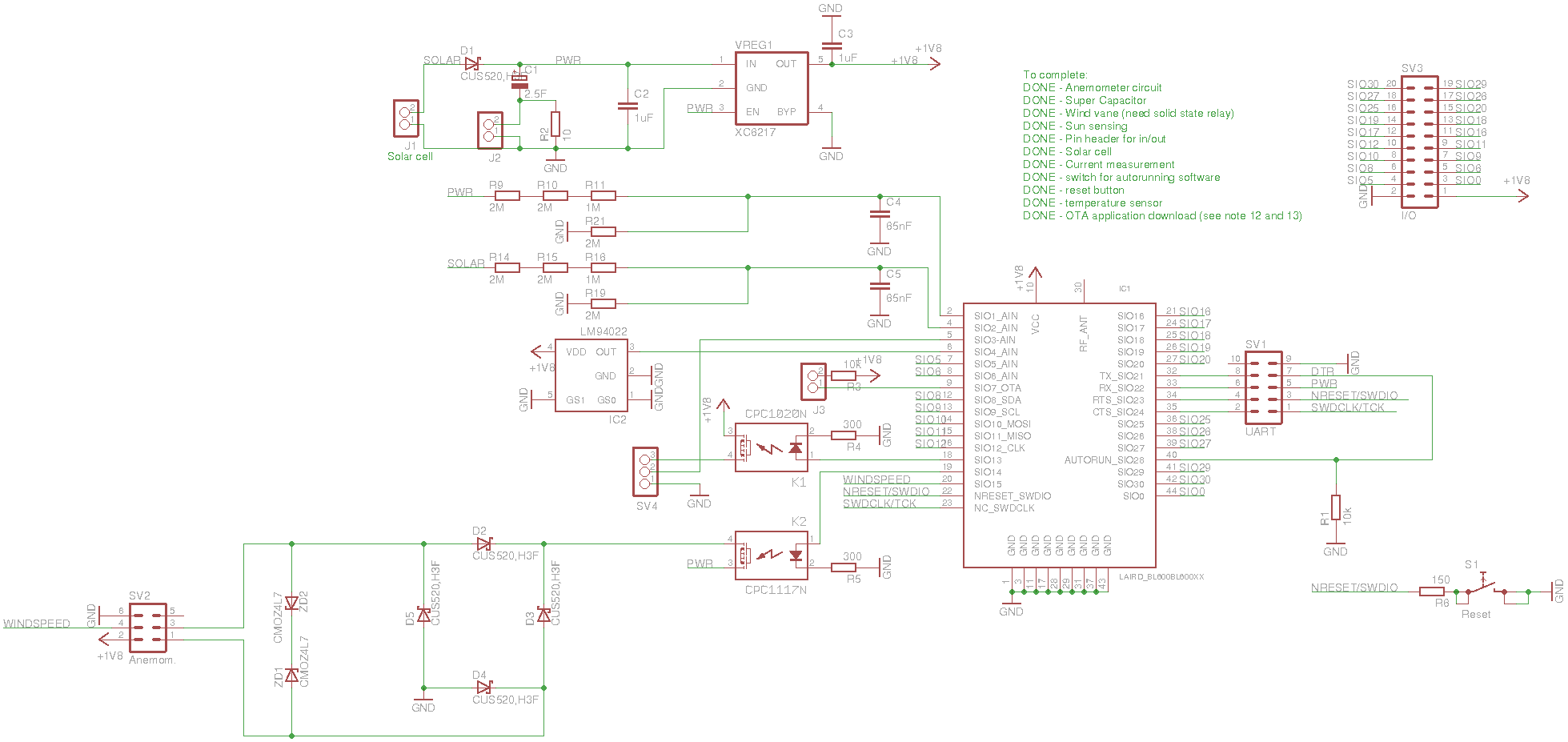
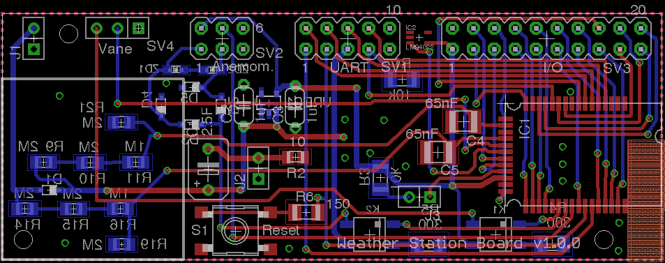
Finally I was able to complete the design of the main PCB I want to use! It is not complex, but since I wanted to make it small and make sure all unused IOs were available for additional external sensors, the routing took some effort.
There are four header pin connectors, with the following functions, starting from the left in the first picture:
- Solar cell (sun sensing and charging)
- Wind vane (wind direction sensing)
- UART (connection to external PCB for UART, JTAG and external power, see older post)
- I/O (Analog and digital lines not already used, to allow add-on sensors)
There is a large area to the left, which is reserved for the super capacitor, and next to it is a reset button (useful if bluetooth connection needs to be reset). I also added a header pin close by to allow current measurement. That will be handy when the current consumptions is to be optimized. The last header pin (J3) is to allow over-the-air update of the software. Can be extremely useful if the weather station is already placed outside.
As always you can find the source files from the git repository link.
(3D pictures below made using online tool at http://mayhewlabs.com/3dpcb)


 Ulf Winberg
Discussions
Become a Hackaday.io Member
Create an account to leave a comment. Already have an account? Log In.