 Alex
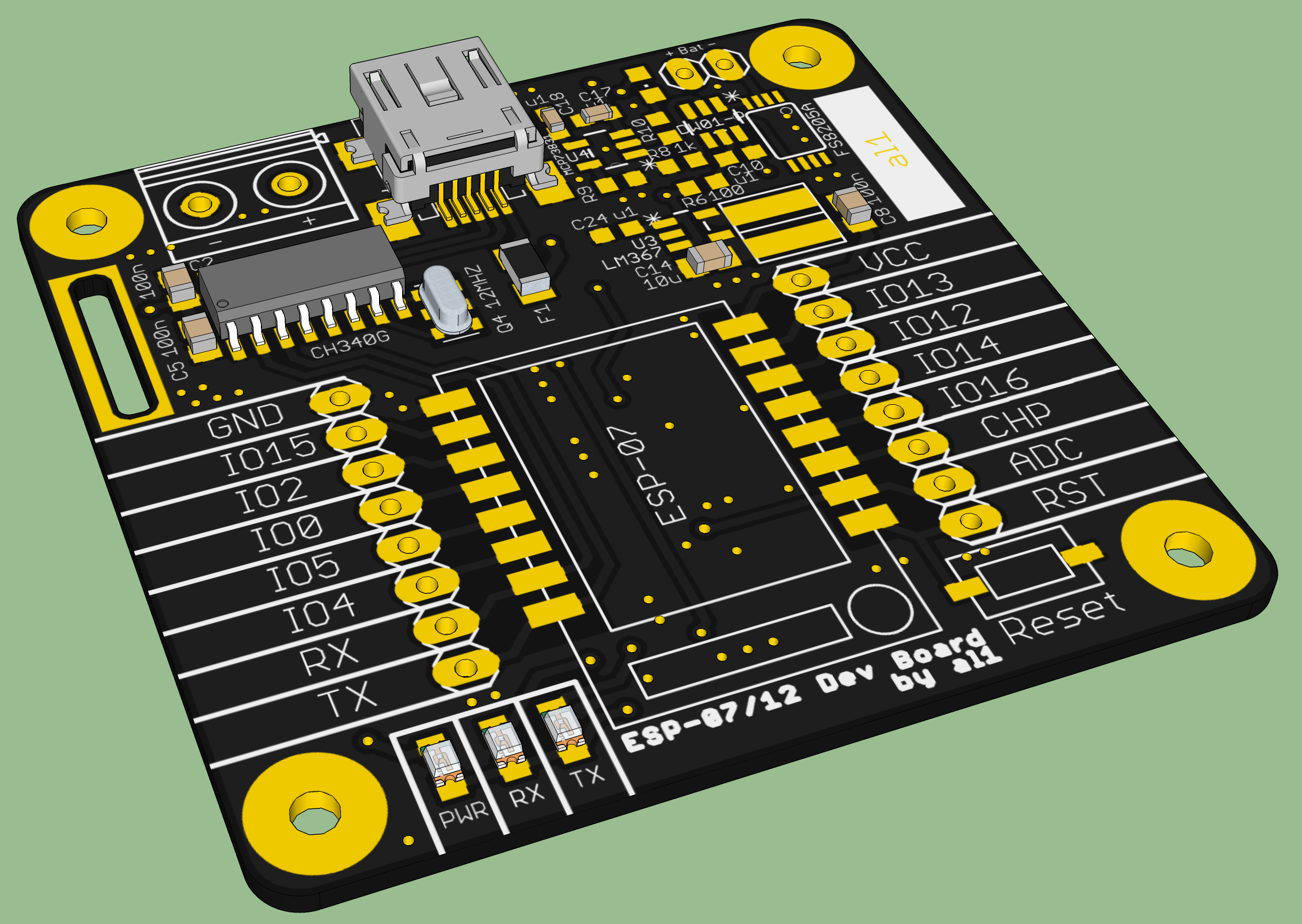
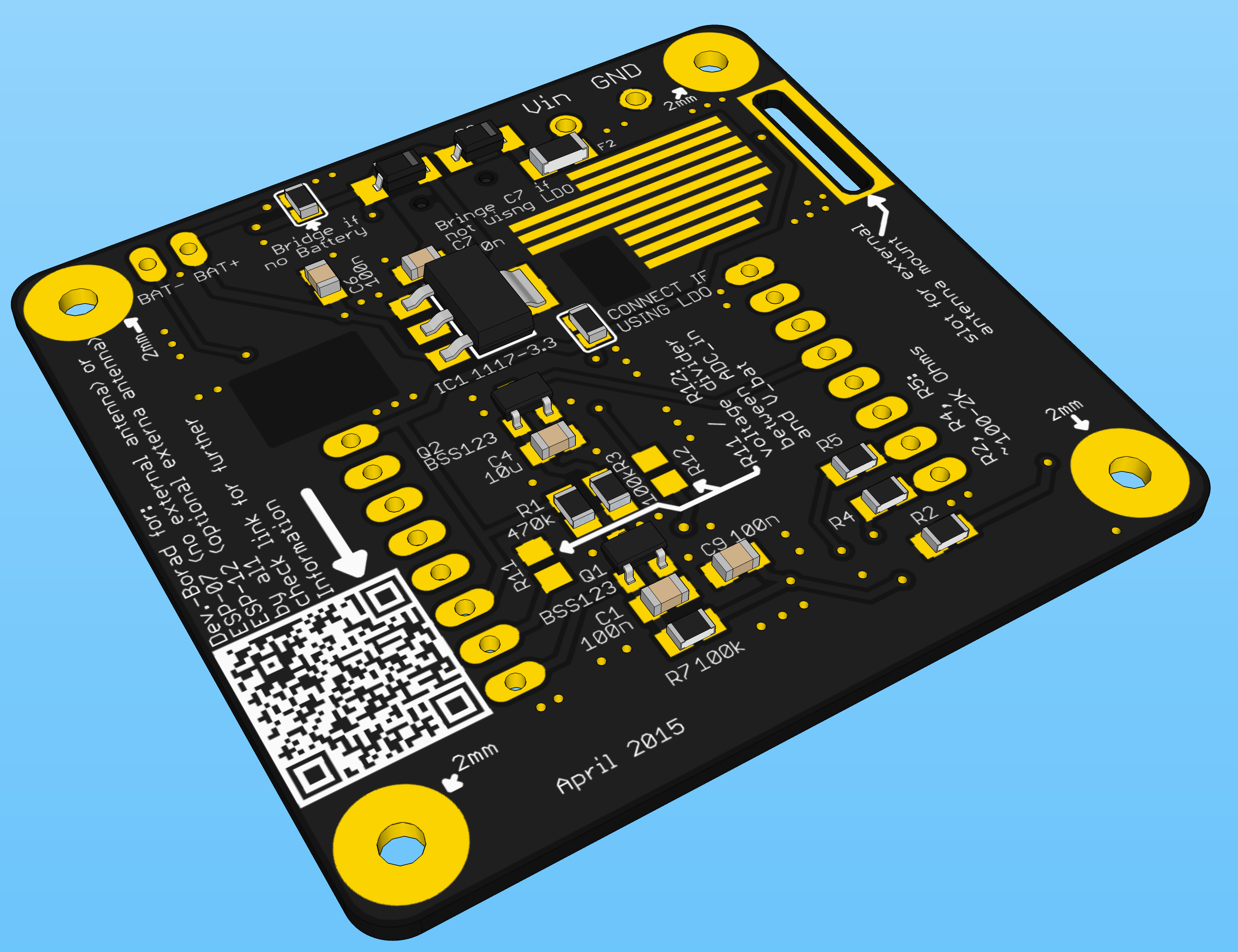
AlexI added some parts to the PCB. So here are some new renderings. I Also decided to use black solder mask, this looks better than the red one (perhaps I will change this again, if the black solder mask is too expensive).
I added some Jumpers for using a linear or a switching voltage Regulator. Also the battery-charging circuit is optional. The renderings show a version with standard LDO (bottom) and no battery circuit.
Top Rendering:
Bottom Rendering:
Discussions
Become a Hackaday.io Member
Create an account to leave a comment. Already have an account? Log In.
I was going to design a breakout board similar to this, but you beat me to it! Awesome, now I don't have to. Any chance of a schematic? Sometimes that's good for spotting obvious errors before you send it off for manufacturing.
One note, too: I don't know if your DRC constraints will allow it, but having a little via on the ESP pads would be good to act as pilot holes. That way you could drill them out a little on one board and install Pogo pins.
Are you sure? yes | no
Thank you for your comment.
I will publish the schematic later. But first I have to tidy up it. I already ordered the first batch of ten boards.
The Idea with the vias in the pads would be a good additional feature.
Specially for a large scale production (i'm not planing this). Maybe I
will do that in Rev2, but I have to check the DRC first.
Are you sure? yes | no