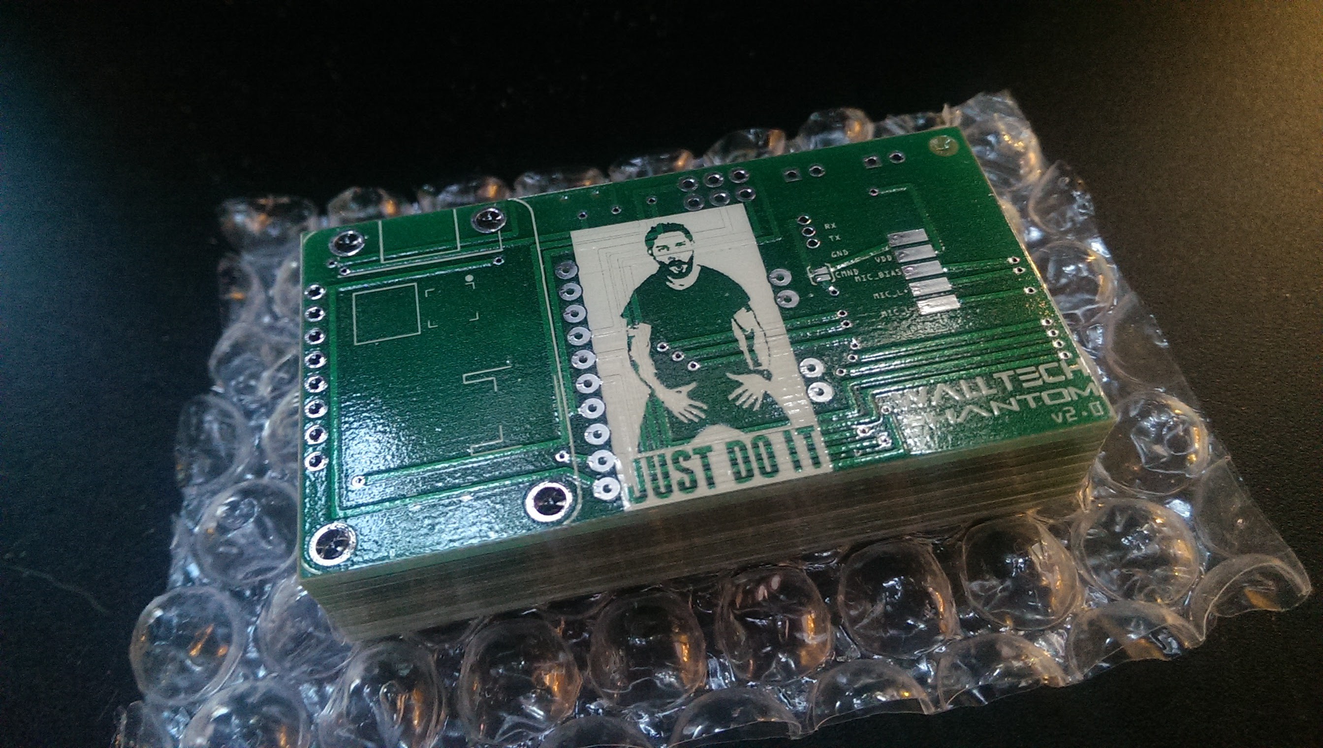
To pick up my PCBs that were perfectly crafted by Bay Area Circuits in Fremont, CA, about an hour away from Stanford, I toured the facility (cheers Brian) and got to see the whole production process as well as the incredible machines that make it happen. It was an amazing tour, and I'll release photos as they are approved by PR for the public.

Finished PCBs: (JUST DO IT!)

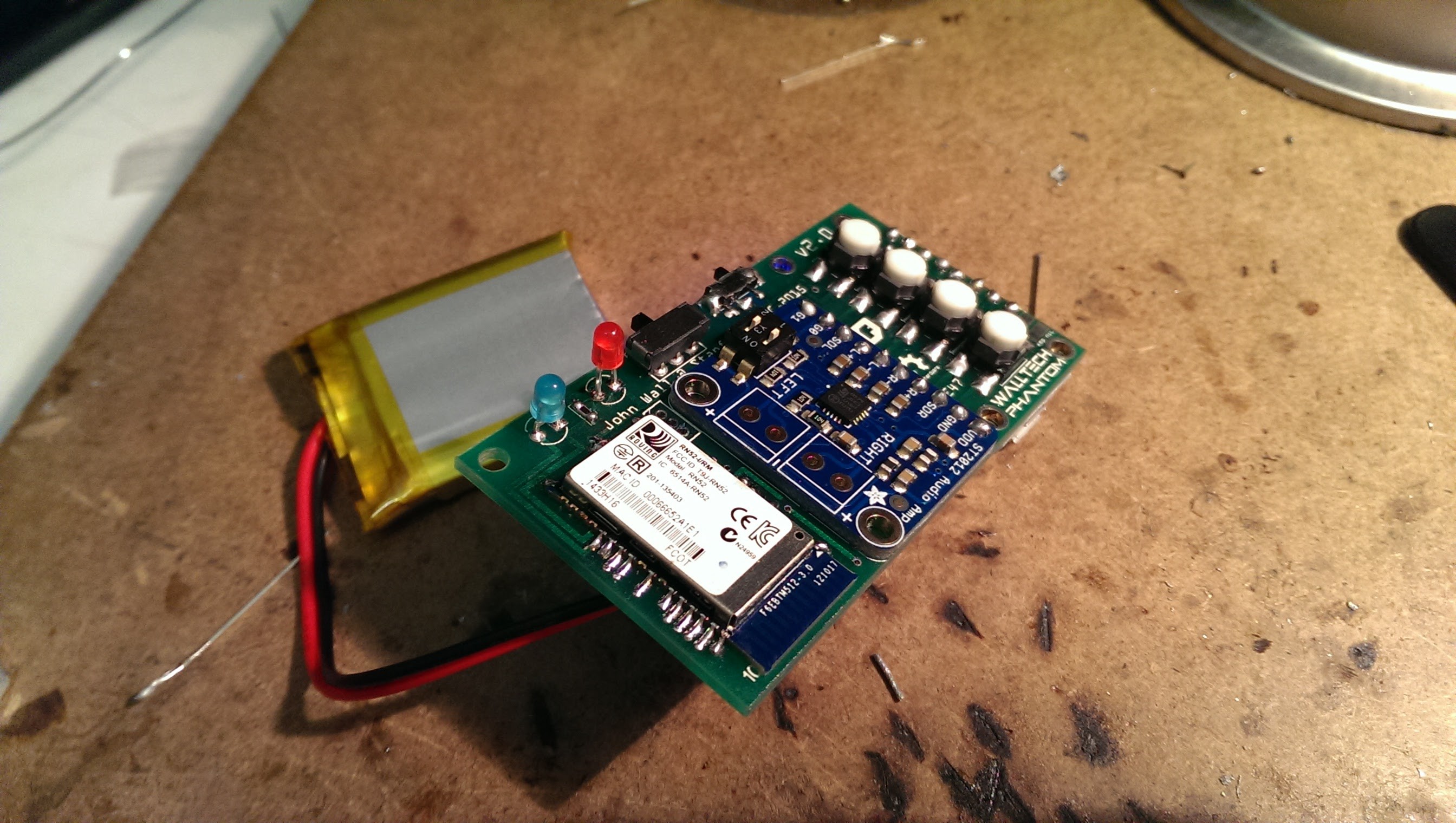
I assembled the first prototype in the Stanford Product Realization Lab (the campus makerspace) and every function of the device worked first time! Here it is! On to the case and final testing!

 WΛLLTΞCH
Discussions
Become a Hackaday.io Member
Create an account to leave a comment. Already have an account? Log In.