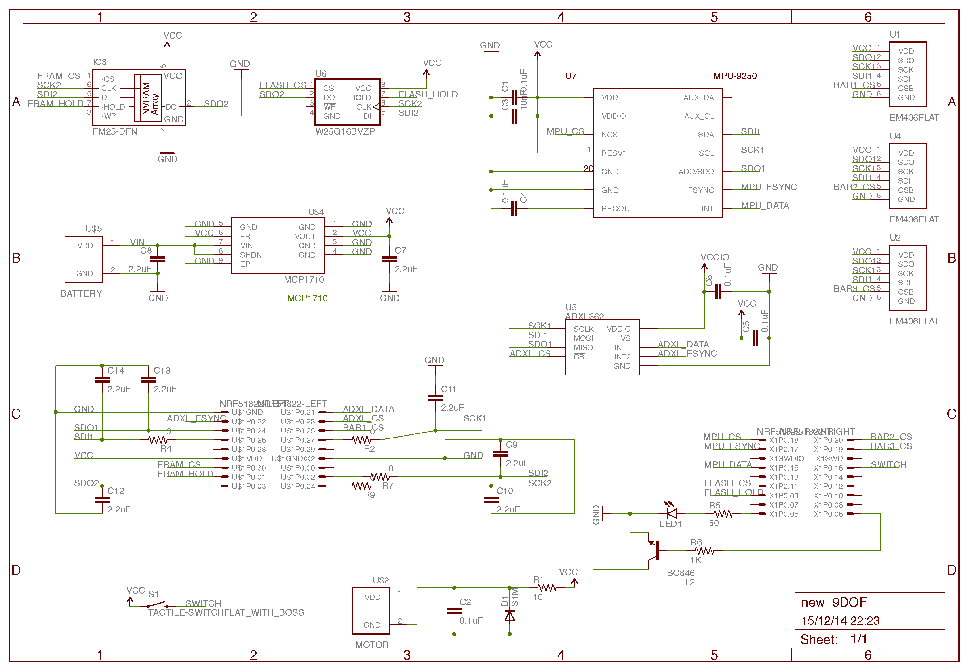
So ... the wheels are turning. We have done the electrical schematics for the board. All measurement components (accelerometer, 9DOF and expansion slots) have been put on SPI1 lane, whereas both FLASH and FRAM memories have been separated onto SPI2. Let's hope we can find room to fit three SPI1 expansion slots for additional sensors.
 Eagle files can be accessed here
Phase 3 - DONE. Now for the tricky part ... squeeze all components on this tiny board. PCB design here we go!
 Lukasz
Discussions
Become a Hackaday.io Member
Create an account to leave a comment. Already have an account? Log In.