Some of the PCBs got lost on the way, but the the decoders and the flipflops work fine. Nonetheless, the project is on hold until they arrive.
I even added some zener diodes to save my LEDs from frying- they suffer from reverse voltage kills thanks the relays. Never thought that the peaks would ever be that huge....
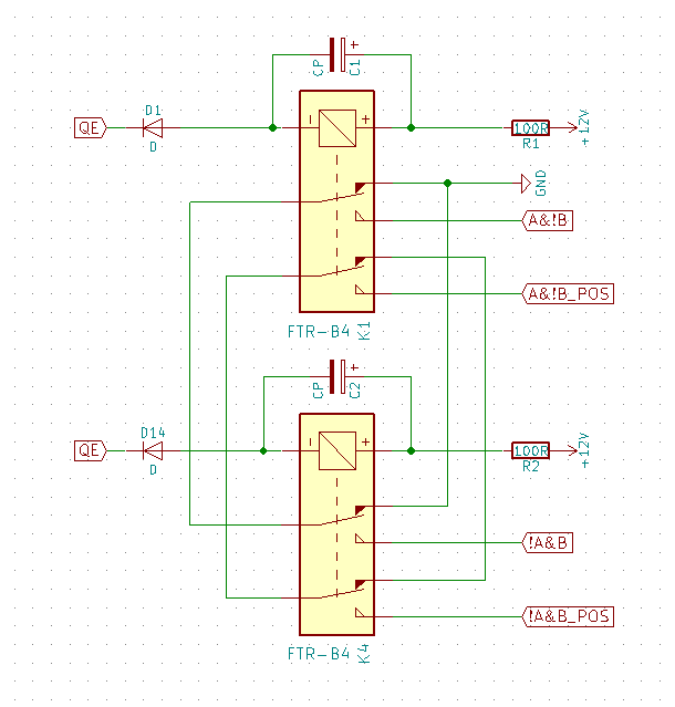
To do at least something I thought that it might be worth it to write a wrap up about my decision to add a A&!B-Gate to every Decoder. The use seems a bit redundant for all non-resetting decoders, but there is a reason to it.
How the clock is carried over in TTL / CMOS
The easiest way to connect one johnson counter to another in a TTL/CMOS world to the other would be to connect the Q (falling clock trigger) or !Q (rising clock trigger) of the most significant FF in the lower stage (faster counter) with the clock of the higher stage (slower counter).
The troubles with the used relay logic
The problem with the existing FF design is, that active outputs deliver an active low (0V) and that the clock signal needs to be 12V -> high. This alone would require a relay to invert the signal. The other thing is, that a very long active high clock consumes #FFx10mA since there is always one of the two input relays closed per FF for a CLK high.
And there is even one more reason to keep the clock signal tristate (not low!) as long as possible:
There are 3 possibilities when a clock signal between counters is active high: ticking (only lowest clock driven by uC), manually setting (2 buttons between dots) and autosetting via the uC. There are several combinations when a clock is set high via the carry-over of a lower stage, neither setting it manually or via uC would work, since something that already is high cannot generate a rising flank.
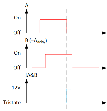
So what was needed was a monostable circuit that generates only one pulse for every input flank. So Q low -> Q tristate would end up in a short "clk tristate - clk 12V - clk tristate".
The design solution
Thanks to the original design from Daniel we have AND gates with A&!B and !A&B Outputs at hand. Using the Q on both inputs and delaying one input generates exactly what we want - a pulse. The delay is easily achieved with a cap and a serial resistor. The resistor is capped by the setting voltage of the relay (9V), but luckily we don't need a very long pulse (setting time ~3ms) so I sattled with 100R and 47uF. 10uF was not enough unfortunately.


Small detail: I planned the inverted output option in in case I would mess up - and I did. But luckily this means now only soldering another jumper bridge together to work. In the video in Log 2 you can see the effect - it generates a pulse at "2->3" and not at "5->0". Fricking inverted logic levels...
 SwiftyTheFox001
Discussions
Become a Hackaday.io Member
Create an account to leave a comment. Already have an account? Log In.