esben rossel
The MCU
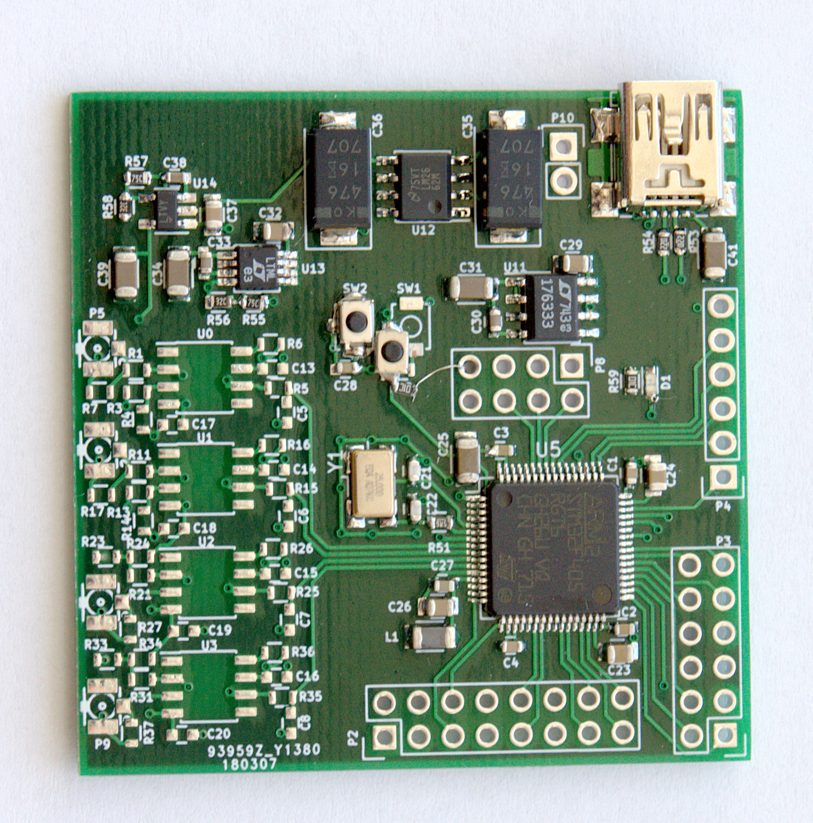
The STM32F405RG was chosen because this is the smallest (physically and computationally) F4 with 3 ADCs, and the only foundation line STM32F4 mcu in an LPFQ64 package. Incidentally, it is also the chip used in the STM32F4stamp which I initially looked to for inspiration.
The MCUs in the STM32F4 family are more or less pin-compatible provided the package is the same, but certain pins may differ eg. Vcap1/2, so other F4's may be used without radical changes to the circuit.
The MCU is connected to a mini-USB B socket and by setting up the microcontroller as a USB-device nothing else should be required for communication.
Another (perhaps more obvious) choice for an MCU for a break-out board with good analogue capabilities would be something from the STM32F3-line.
The opamps
The ADCs of the STM32F405 have 12-bit resolution and a range from 0-Vdd. They can run at full speed (36MHz) when the supply voltage is between 2.4V and 3.6V. This circuit provides a Vdd of 3.3V meaning the ADC-range is 0-3.3V.
To utilize the full range of the ADCs the analog input will most likely need conditioning ie. scaling (gain) and level shifting. The PCB provides two inputs through AD8027 opamps in inverting and non-inverting mode respectively.
Inverting mode:
The schematic for the inverting opamps is (in brief):

The gain is:
G = - R₂/R₁
The level shift is:
S = R₄/(R₃+R₄)·(1+R₂/R₁)·Vref
The output voltage is:
Vout = G·Vin + S = -R₂/R₁·Vin + R₄/(R₃+R₄)·(1+R₂/R₁)·Vref
The PSU for the analog section delivers ±4.65V, and Vref is connected to +4.65V.
Non-inverting mode:
The schematic for the inverting opamps is (in brief):

The gain is:
G = (1 + R₂/R₁)
The level shift is:
S = -R₂/R₁·Vref
The output voltage is:
Vout = G·Vin + S = (1 + R₂/R₁)·Vin - R₂/R₁·Vref
The PSU for the analog section delivers ±4.65V, and Vref is connected to a voltage divider between -4.65V and +4.65V.
My initial choice for the opamp was the AD8021, but simulations in LTspice indicated that Vout wouldn't be able reach 3.3V with this particular chip even when bypassing the LDOs to get a ±5V supply. The AD8027 is a rail-to-rail high-speed precision opamp used for 16-bit ADCs and does not have this problem, but depending on the signal-range the select pin should either be floating or connected to V+ to avoid having the opamp's crossover point in the signal. Refer to the datasheet.
The power supply
The circuit is powered from 5V USB. The digital and analog parts of the circuit have separate supplies.
The supply for the MCU is handled by a LT1763 (3.3V 500mA) low-noise LDO.
The dual supply for the opamps features a LM2662 voltage inverter (200mA) and two low-noise LDOs. One negative (LT1964) and one positive (LT1962), who each deliver
Vout = ±1.22V(1+R₂/R₁) = ±1.22V(1+59k/22k) = ±4.65V
The LDOs noise-levels are in the range 20-30µV, well below the ADC's tolerance for the LSB:
3.3V/2¹² = 0.81mV
Available GPIOs
The circuit board is for an STM32F405 in a LQFP64 package, so not every GPIO is exposed and furthermore not all pins are broken out. Still, with the chips alternate function mapping, most peripherals should be accessible. Here's the list of the accessible pins:
Dedicated analog input
PC0 - PC3
... Read more »