 Crypto [Neo]
So I'm about 98% done with the PCB routing, I took a lot of time to experiment with different routings for the bus lines to find a design that would allow me the most possible space for the rest of the components. I started with a ratsnest like this
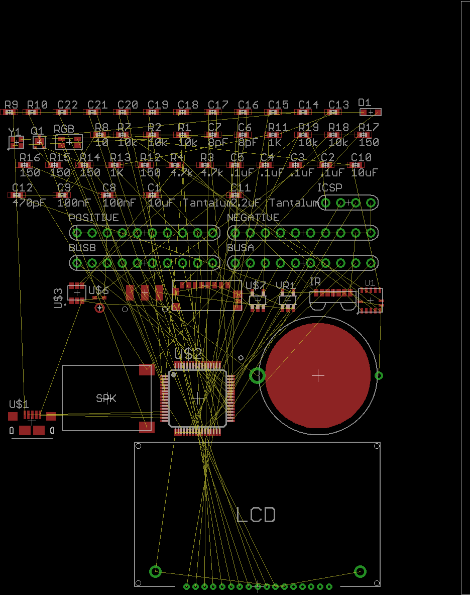
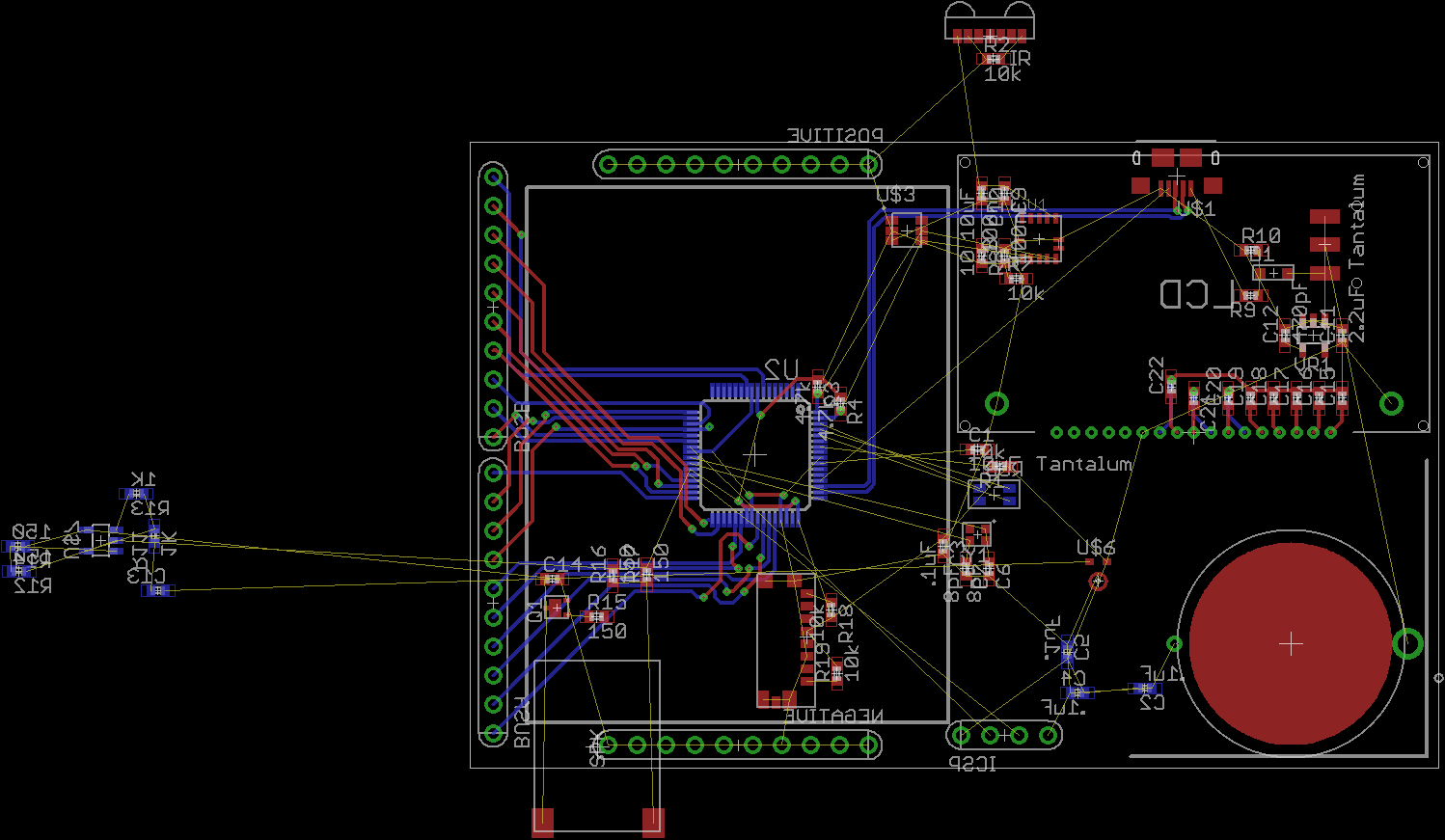
And reorganized components and the bus lines into a nice configuration that groups the ICs with their resistors and capacitors. At this point in the design I'd found the bus line configuration that I was happy with:
Timestamp: ~`18hrs in
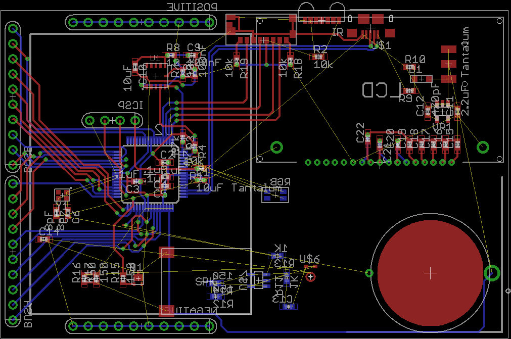
And finally routing everything else into place. The fun thing is that usually during this process stuff gets moved around into even better configurations. Once the initial routing is complete we can go back over it and compact everything a bit.
TImestamp: ~20hrs in
This was actually a nice challenge to route because I have so much damn space to work with!! I'm so used to be space constrained that actually having so much freedom is actually a hindrance!
Anyways, it's break time for dinner. I haven't be able to really focus on this thing today, which is why the updates have been so sporadic (and why the PCB isn't done yet!) but afterwards I'll be able to actually get some real work done :D I'll be really surprised if the PCB isn't finished by midnight. Then I can focus on adding a few things I'd like to see, and actually keeping tabs on my progress.
Discussions
Become a Hackaday.io Member
Create an account to leave a comment. Already have an account? Log In.