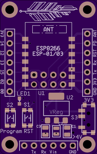
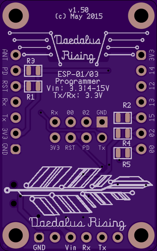
Well, after fixing the ground plane issue, I decided to make major revisions to the layout and labeling of my board, creating a higher-quality, more useful board in the process.
First, an obligatory changelog:
- Remove ground plane under antenna
- This was previously addressed in my last post. But here it's actually complete!
- Change size of board to 1.0"W by 1.6"L.
- This was to accommodate the full length of the ESP-01 board, which would previously just out over the edge of the board. I decided that this would add robustness for a marginal loss of size and cost (the cost is an extra $0.30 per board at OSH Park).
- Change to layout of components.
- This was partly in response to the changed board size, but also just to make it easier to solder and visualize the path of everything on the board. Additionally, this meant fewer vias, and a cleaner look overall, with more open space.
- This also allowed more space for...
- Mounting Holes. For number 2 standard sized US screws (0.090" hole).
- I think this will allow my board to be more useful in a variety of different projects, and allow for permanent standalone installations.
- Label switches with their function, and S3 with the direction for each input voltage level
- Labels for ESP-01 Headers
- Clearer Logo Graphics.
- Cause as much as I love pixel art, I love for my work to be at a higher quality even more.
Renders
 ^Top
^Top
 ^Bottom
 drewrisinger
Discussions
Become a Hackaday.io Member
Create an account to leave a comment. Already have an account? Log In.