 drewrisinger
I was really fortunate to have access to my school's manufacturing equipment in constructing my case, even though I'm an Electrical Engineering major.
I was able to construct a case in two parts, with some assistance on the CAD side.
Bottom Part
The 3D printed bottom.
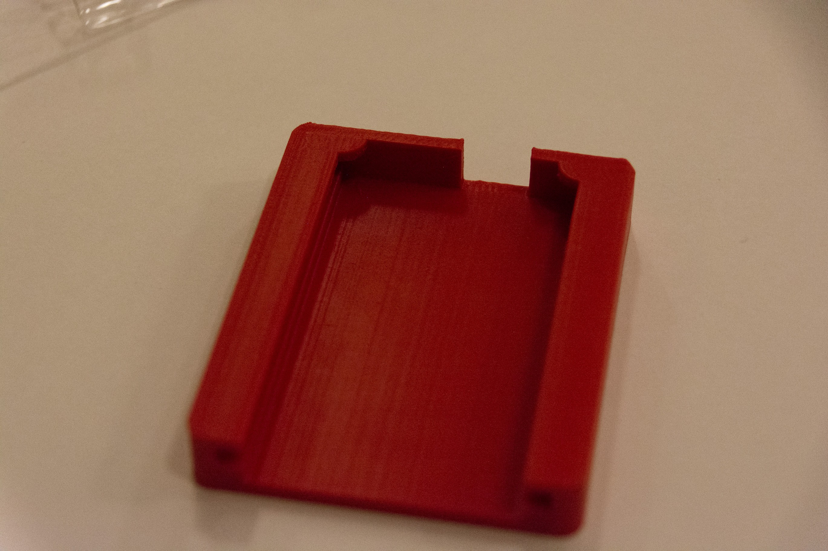
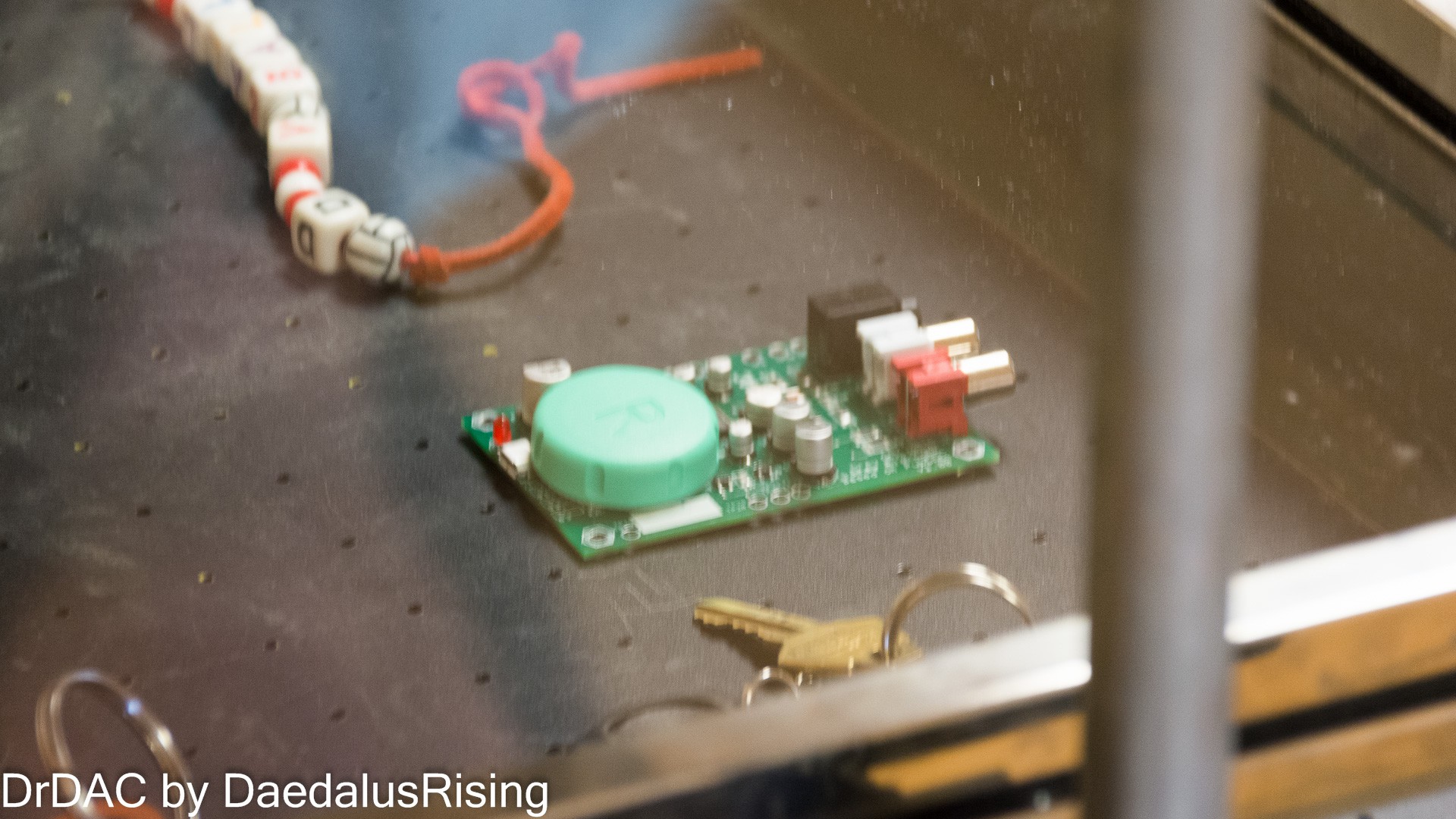
This is a fairly simple part, just printed on a 3D printer. The circuit board slides into a slot beneath the top edge, and there's an opening on the back edge for the USB port. While the tolerance for the height of the circuit board opening could've been lower, it wasn't bad for a rev 1.0
Top Layer
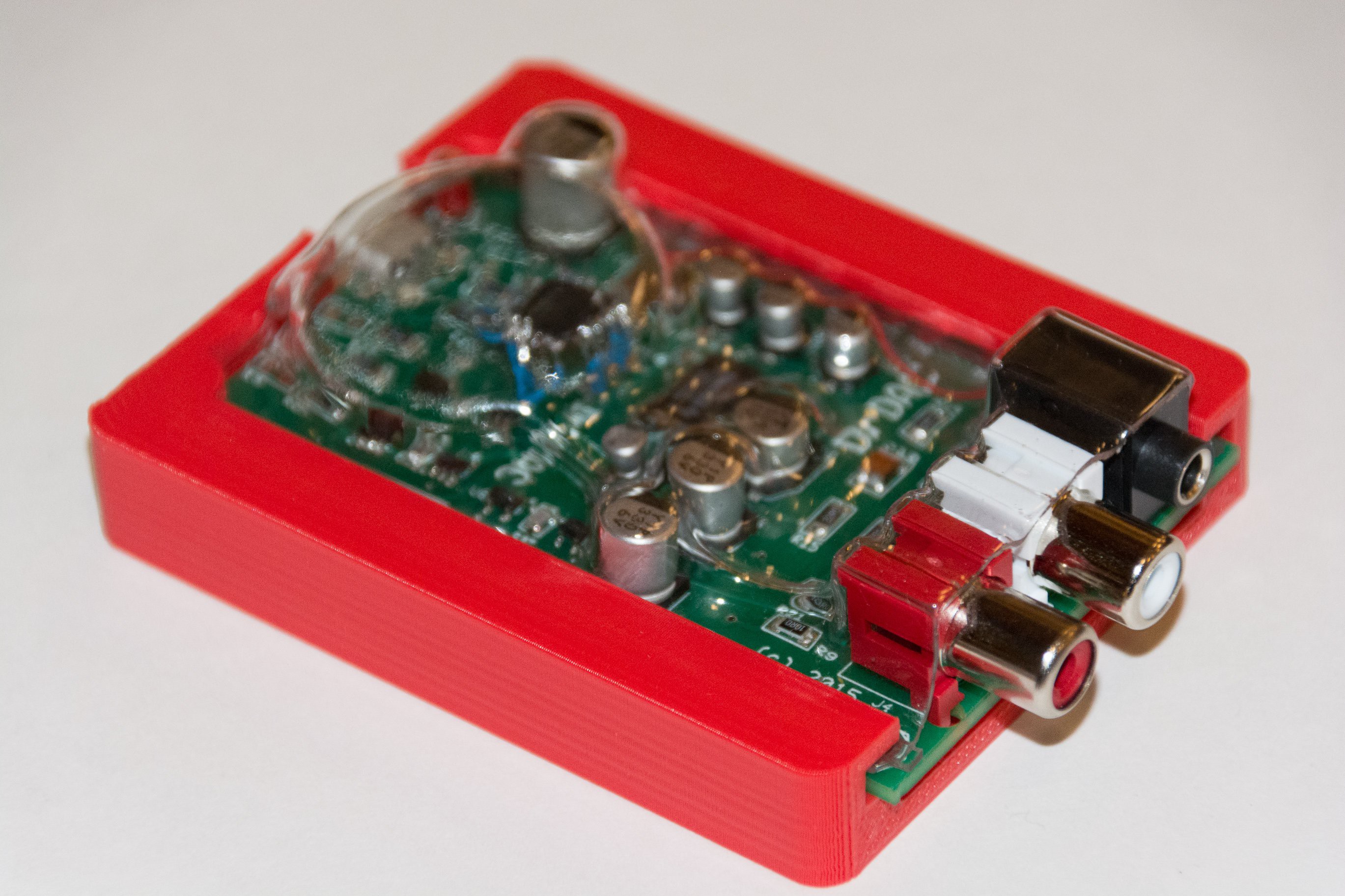
The top layer was made from vacuum-formed plastic (or thermoformed, depending on who you ask).
 The bubble on the right was made by a contact lens cover, which served to protect the delicate soldering work of my problem IC from being destroyed in the vacuum-forming process.
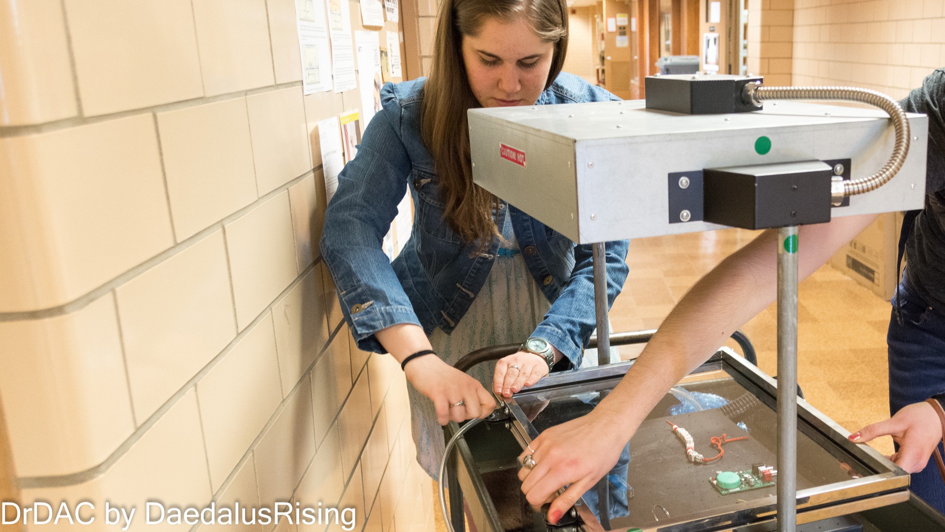
Learning to use the Thermoforming Machine (from the mechanical engineers):
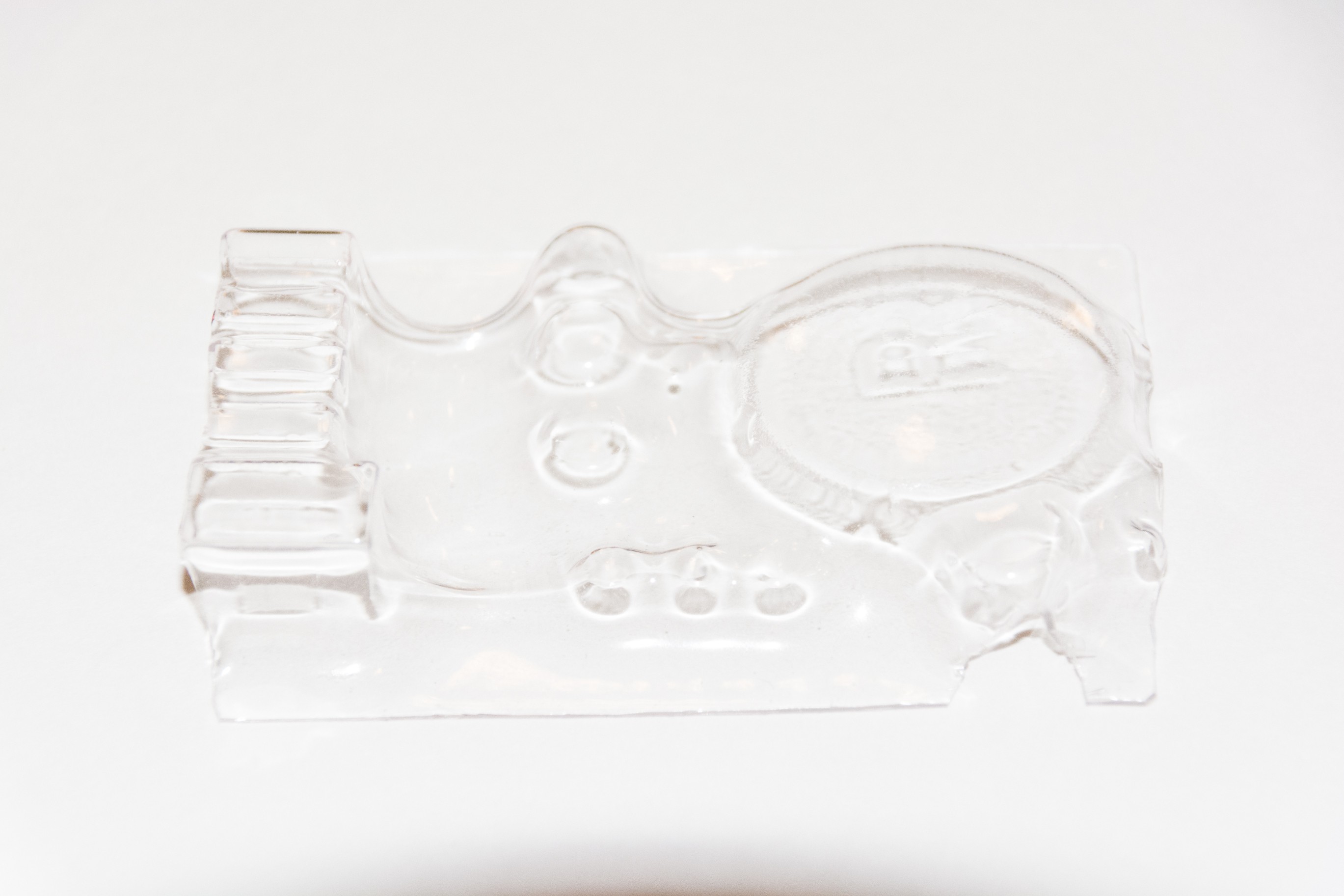
 Post-thermoformed
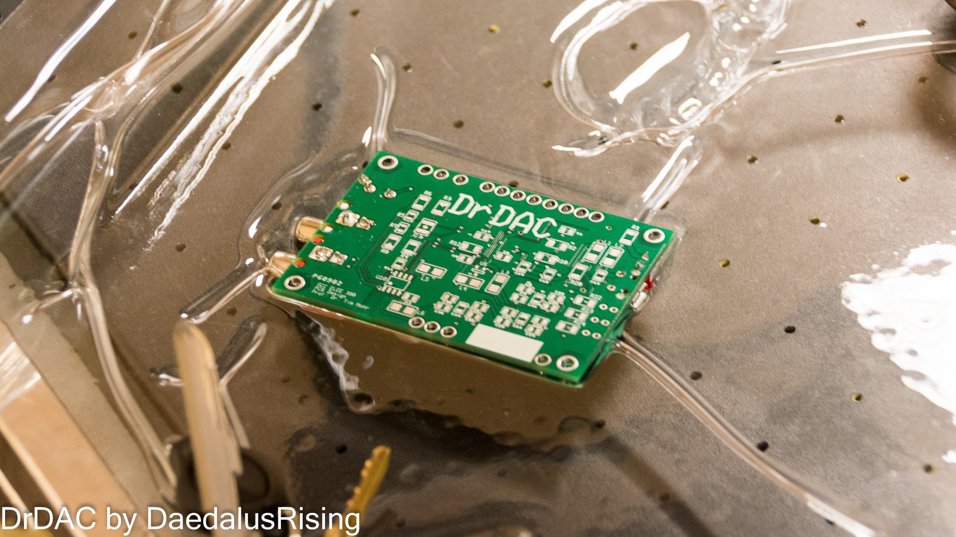 With just a little bit of cutting, I had a sweet custom-fit case to protect my components!
Discussions
Become a Hackaday.io Member
Create an account to leave a comment. Already have an account? Log In.