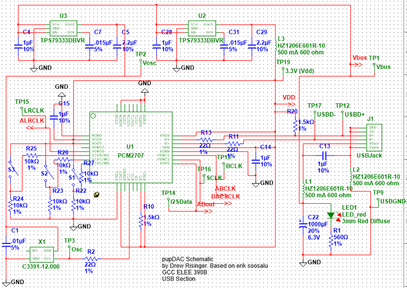
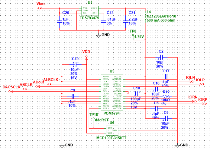
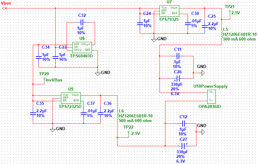
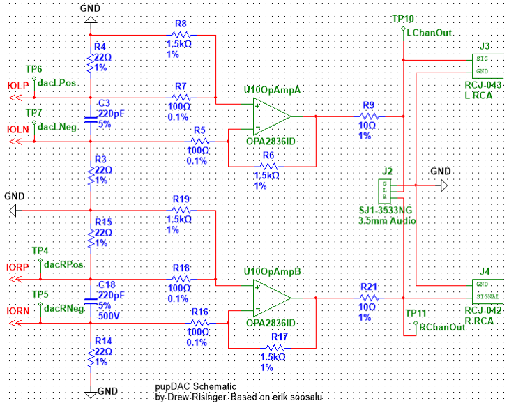
This is the schematic that corresponds to version 1.0 of my design. It's divided into 4 sections: the USB section (which takes USB signals in, and outputs I2S Data), the I2S DAC (which outputs a balanced audio signal), the output opamp power supply section, and the opamp circuit itself, which provides the output.
USB Section

I2S DAC

Opamp Power Supply

Opamp Audio Output

 drewrisinger
Discussions
Become a Hackaday.io Member
Create an account to leave a comment. Already have an account? Log In.