Close
0%
0%

Beckman DU 600 Reverse Engineering

Reverse engineering process for a 68332 based system

Similar projects worth following
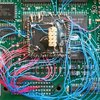
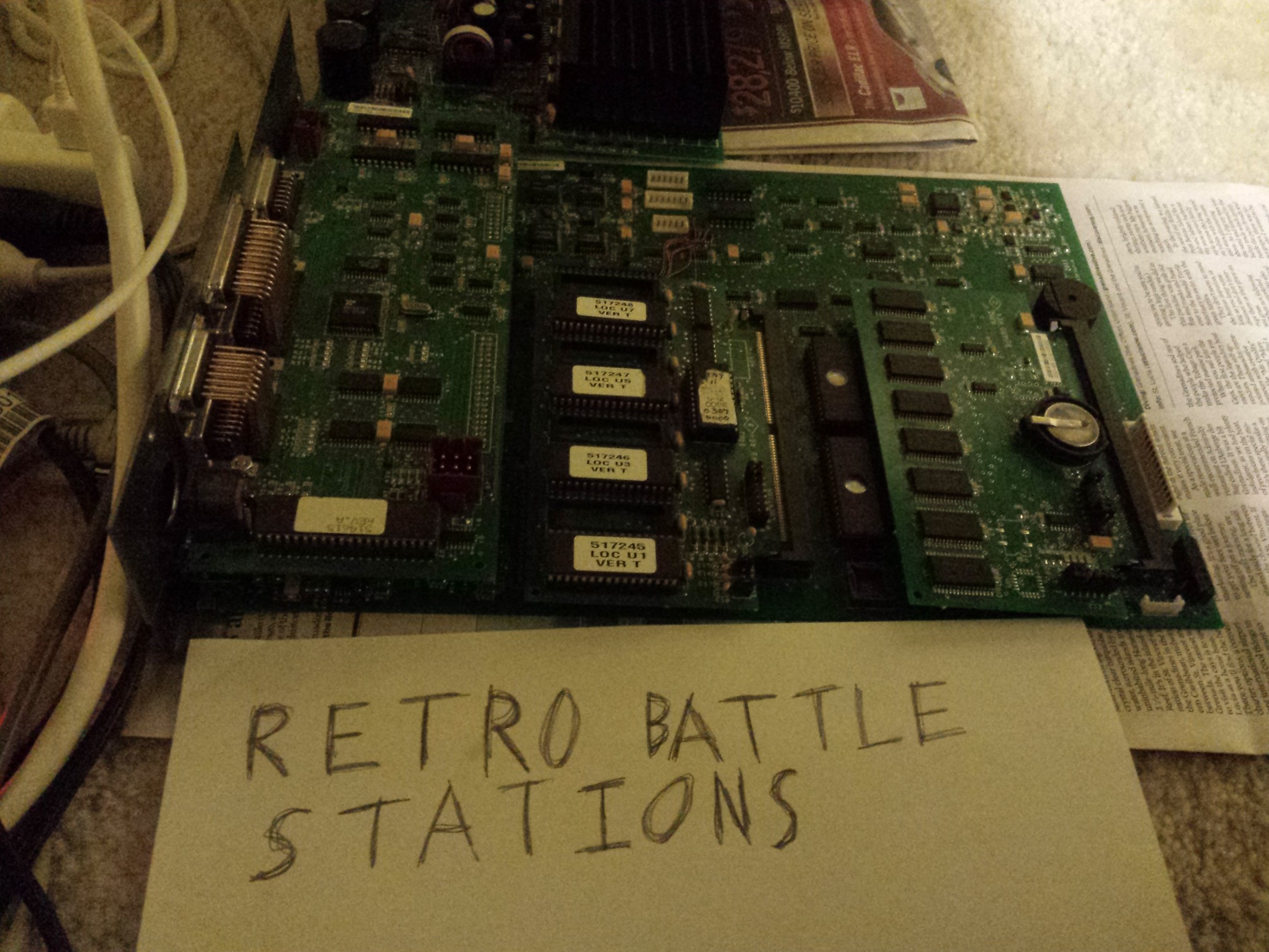
Late 2014, I found a Beckman DU600 spectrophotometer in the trash. I took a quick look at the back and saw a VGA port, some serial ports, and a parallel port, so I decided to take it. Upon disassembly, I saw that the motherboard of the unit was based around the motorola 68332 microprocessor. It had 1MB onboard ROM, 512K ROM in an addon card (with sockets on that card to increase to 1MB), 256KB battery backed SRAM onboard, 1MB battery backed SRAM on a card, an Epson RTC chip, 1MB of DRAM, 512KB of video RAM for the onboard SVGA controller (Cirrus Logic CL-GD5429), discrete logic for a printer port (IEEE 1284), 1 onboard DUART, 1 more DUART on a daughtercard, and an AT keyboard controller chip (a real live NEC 8741, similar to the intel i8042 used in IBM PC/AT's). In addition to all of this (as if the system wasn't capable enough already) there's plenty of motor drivers, special stepper motor control circuitry, general purpose I/O lines, at least one DAC and a dual ADC.

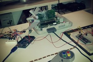
I have been reverse engineering the hardware of this 68332 based system in order to run my own software on it. What that software will be specifically, I don't exactly know yet.

This is a link to all of the pictures:

Beckman DU600 pictures

Note: many of these pictures are quite large, up to about 5MB

Here is copy and paste from the text file I use to document anything I reverse engineer from the hardware:


default setup of address space
this could change if software changes it


$00 0000 - CSBOOT, 1MB, onboard boot ROM
$10 0000 - CS0, 1MB, card 1 & 2, addon ROM card
$40 0000 - CS1, 1MB, card 3 & 4, onboard DRAM
$5C 0000 - CS8, 256KB, card 8, onboard SRAM
$60 0000 - CS2, 1MB, card 5 & 6, SRAM card
$B0 0000 - CS7, 1MB, 8 bit port, videochip
$D0 0000 - CS5, 16KB, I/O
$E0 0000 - CS9, 2KB, 8 bit port
$F0 0000 - CS10, 64KB, 8 bit port, I/O
$FF E000 - TPURAM, 2K
$FF F000 - internal CPU on-chip registers


CS5 controls U210, a 74AC138 for address decode
CS9 goes to a pin on J3, and nowhere else as far as I can tell.
CS10 goes to U25, a 74AC138 for address decode. also goes to pin on JA1 for daughterboard.


hardware I/O addresses:


CS5:0-7FF - UART1
This is the base address for the 68C681 on the mainboard. The base set of registers is repeated to fill the block of addresses.


CS5:802 - LEDS - doesn't clear IRQ
CS5:800 - PPORT - clears IRQ
This write address controls the parallel port output pins and the 4 onboard LEDs. Bit 15, 14, 13, and 12 control CR 50, 51, 52, and 53 respectively. Bit 11 controls the /SELECT_PRINTER line. Bit 10 controls the RESET line. Bit 9 controls the /LF line. Bit 8 controls the /STROBE line. The lower 8 bits control the data outputs. This address is repeated in the range 800-FFF everytime ADDR2 is 0. If any address in this range is read or written which has ADDR1=0 then the /ACK interrupt is also cleared.


TODO: figure out how to read the status lines for the parallel port, should be U57


CS5:1800-1FFF - J4


CS5:2000-27FF - RTC
Base address for Epson RTC registers


CS5:2000-2800 - EEPROM


CS5:3800-3FFF - DRAMC_CNTL
This address is used to write U719 (74AC573), an 8 bit latch. The actual chip seems to have the data lines hooked up backwards from the numbering in the datasheet, and it's attached to the high bits of the CPU data bus. The output of this latch is enabled or disabled by TPU channel 15. A 0 on the TPUCH15 pin on the 68332 enables output from this latch. Bit 6 and 7 appear to be unused. Bit 5 controls the DRAM controller /DISRFSH line. Bit 4 controls the DRAM controller /ML line. Bit 3 and 2 go to the PSU connector. Bit 1 and bit 0 seem to mask interrupt sources from the power supply board. A 1 masks the interrupts. The interrupts share a single interrupt latch flip flop and use IRQ1. They are cleared by a reset or reading this address.


CS7:0-FFFFF - ISA bus/SVGA controller
The SVGA controller is mapped here. 0-7FFFF seems to be mapped to I/O reads and writes (not confirmed) while 80000-FFFFF seem to be mapped to memory reads and writes. This is necessary because the video chip is made to work on an ISA bus which has separate memory and I/O spaces while the 68K does not.


chip is setup for MCLK on MCLK pin
ISA bus
Symmetric DRAM
single WE, multiple CAS
6 MCLK RAS cycle
44.74431MHz MCLK
32K ROM BIOS at C0000-C7FFF
8 bit BIOS ROM
Internal MCLK
3C3h is video system sleep register


CS7:02000-02007, 02406-02407 - ATA registers
This is piggybacked into the pseudo ISA bus used for the VGA controller. Decoding is done using a 74ACT138 decoding the top 6 address lines (A15-A10).


CS10:0-3FF - UART2
This is the base address for the 68C681 on the daughtercard. The base set of registers is repeated to fill the block of addresses. This also reappears at 2000-23FF


CS10:400-7FF - KB controller
odd addresses are status/command, even addresses are data. These registers may be repeated at 2400-27FF


CS10:800-BFF - MTR_CNTRL
This address writes to U18 (74AC573) on the daughtercard. It's bits control various motor functions on the daughtercard. Bit 7 seems to be disconnected by a jumper....

Read more »

hardware.txt

description of hardware on the board

plain - 8.67 kB - 12/23/2016 at 00:07

Download

  • fast 68000 block memory move routine comparison

    joe.zatarski07/12/2017 at 02:37 1 comment

    OK, I guess I'll do another log since all I have to do is copy and paste some stuff from a reddit post: https://www.reddit.com/r/m68k/comments/63ov3e/fast_68000_block_memory_move_routine_comparison/

    simple memory move routines based around MOVE and DBRA are often regarded as fairly fast on the 68000:

    .loop:
        MOVE.L  (A0)+,(A1)+ ; do the long moves
        DBRA    D0,.loop
    

    This runs decently fast on the 68000, a bit faster on the '010 and above due to the fast loop feature they added for DBRA, especially if your RAM is otherwise slow. However, it's not the most efficient way for the '000, or the '010, and certainly not the higher variants of the 68000.

    Enter the MOVEM instruction. This single instruction is capable of loading up to 16 long words, with only the instruction overhead fetch of a single instruction. The problem? You can't use the postincrement mode for the destination, only the source, so you have to manually (in a separate instruction) add to the destination pointer. Additional complications include that using the stack pointer or your source and destination pointers to hold data within a MOVEM are probably not a good idea:

    MOVEM.L (A0)+,D0-D7/A0-A6 ; not a good idea, unless you're sure this is what you want. behavior varies by CPU
    

    So in reality, assuming you don't want to use your stack pointer either (also not a good idea if you're running in supervisor mode especially) you should set aside 4 registers, one for source, one for destination, your stack pointer, and a loop counter.

    Anyway, I started getting curious whether or not a MOVEM based routine would be faster than a simple MOVE; DBRA like the first example. The MOVE; DBRA has virtually no instruction fetch time, but the MOVEM routine has less loop overhead due to transferring large blocks per loop iteration rather than a single byte/word/long. I decided to run a test on real hardware. I set up the routines shown below to transfer a 256K block 256 times, and timed them with a stop watch. A stipulation on either routine is that they must have word aligned source and destination.

    ; 68K block memory move using MOVEM
    ; this routine is roughly 2.5x faster on a motorola 68332 running out of its fast 2-cycle TPURAM
    ; the test was performed by moving a 256K block approximately 256 times (might have been an off by one in there.)
    ; the block was moved from SRAM to SRAM each time by each routine. Both routines ran out of fast 2-cycle TPURAM.
    ; in theory, the above doesn't matter much for the 2nd routine, since should run entirely in the special loop mode.
    memmovem:
    ; parameters:
    ; A0 - source (word alignment assumed)
    ; A1 - destination (word alignment assumed)
    ; D0 - size in words (0 is undefined)
    
    ; variables
    ; D0 - size in MOVEM blocks (rounded down)
    ; D1 - number of words not included by above
    ; D1 - reused for MOVEM
    
        DIVUL.L #24,D1:D0   ; 22 words per MOVEM
    
        SUBQ    #1,D0   ; needed for the way DBRA works
        SUBQ    #1,D1
    
        BMI .loop   ; if D1 negative, we happen to have round number of MOVEMs
    
        LSR.W   #1,d1   ; convert from word count to long count
        BCC .longloop
    
        MOVE.W  (A0)+,(A1)+ ; correct for word
    
    .longloop:
        MOVE.L  (A0)+,(A1)+ ; take care of long moves first
        DBRA    D1,.longloop
    
        JMP .loop
    .outerloop: ; do MOVEM sized moves
        SWAP D0
    .loop:
        MOVEM.L (A0)+,D1-D7/A2-A6   ; 12 long words
        MOVEM.L D1-D7/A2-A6,(A1)
        ADDA.W  #48,A1
        DBRA    D0,.loop
        SWAP    D0
        DBRA    D0,.outerloop
    
        RTS
    
    memmove:
    ; parameters:
    ; A0 - source
    ; A1 - destination (word alignment assumed)
    ; D0 - size in words (0 is undefined)
    
        LSR.W   #1,D0   ; convert to long count
        BCC .longloop
    
        MOVE.W  (A0)+,(A1)+ ; correct for word
        jmp .longloop
    
    .outerloop:
        SWAP    D0
    
    .longloop:
        MOVE.L  (A0)+,(A1)+ ; do the long moves
        DBRA    D0,.longloop
        SWAP    D0
        DBRA    D0,.outerloop
    
        RTS
    

    These routines were run from inside my 68332's TPURAM, a very fast 2-cycle SRAM internal to the 68332. This reduced instruction fetch times for the MOVEM routine as much as possible, and is not an unreasonable purpose to use the RAM for, in my opinion....

    Read more »

  • Multiuser Timesharing EhBASIC

    joe.zatarski07/12/2017 at 02:31 0 comments


    This was just a quick project I cranked out as a proof of concept, mostly, that I could figure out a preemptive multitasking system at a very simple level. Basically, I took Lee Davison's EhBASIC for MC68K (RIP Lee Davison), which I had previously ported to my board, and I ran 4 instances of it task switching 64 times per second. Each instance used it's own serial port. The threads each run in user mode, and the supervisor implements a simple TRAP API for I/O, choosing the serial port based on the process ID. When the 64hz timer interrupt fired, I would save the context, load the next one, and then resume based on the new context. This is the only way a process releases control in this simplified system. There is no way to give up control early, not even when a blocking I/O call is made. Like I said, it's just a proof of concept. Due to the way Lee Davison wrote EhBASIC, the code is position independent, and it also accepts a pointer and a size to tell it the region of memory to use. No addresses are hardcoded, everything is a relative address. This makes it particular easy to do this with, since I can use the same code segment for each instance, and all I have to do is supply a different RAM region for each instance. I believe I divided a 1MB block of RAM into 4 256K blocks, with each instance of the BASIC interpreter using one block. Lots of things in my multitasking system were hardcoded and fixed. It is fixed at 4 processes, has memory for the 4 contexts statically allocated, etc., but it served fine as proof of concept.

  • Joe-Mon Wins at HackIllinois

    joe.zatarski07/12/2017 at 02:14 0 comments

    TL;DR: participated in hackathon, worked on Joe-mon, didn't expect to win, won '1517 Grant Prize'. https://www.facebook.com/hackillinois/posts/1360661100660096:0

    https://devpost.com/software/joe-mon

    Well, this is old news considering HackIllinois was back in February, but better late than never I suppose.

    HackIllinois is a Hackathon, if you don't know, where college students get together for a weekend and just 'hack' as they call it. Being an Electrical Engineer, I've always been more involved in the hardware side of things, but obviously I like to delve into the software side as well. My first year participating in HackIllinois, I took a crash course in FPGA's and Verilog, and attempted to create an exact clone of the Atari arcade game 'Breakout' in Verilog (the game was entirely TTL originally, no software or CPUs). By the end 60 hours of work, I was exhausted, and I also had what appeared to be a nearly functioning game, but I was having some issues. I later realized that I had far more issues than I realized at the time. As it turns out, you can't trust everything you find on the internet, and the Verilog replacements for 74-series logic I obtained online weren't actually correctly implemented, causing a myriad of issues.

    The next year, I participated again. This time, I was working on the Beckman DU600, attempting to port the operating system from 8 bit Atari computers (the 400/800/XL/XE line) to the 68K running on the board. This was way too large of a project, and to make matters worse, the HDD on my laptop began crashing halfway through the weekend, so I had to go back to my apartment to begin the process of saving what I could, while I could. I never did lose any data from that, but I did eventually replace the HDD. 1TB HGST drive with a 3-year warranty. Hopefully this one will last, because otherwise there are no decent consumer HDD manufacturers left in the world. Not for spinning rust anyway....

    This last year, I set out to work on the Beckman DU600 again, this time continuing work on Joe-Mon. I was working hard, at the time, on implementing a disassembler. Most of this was admittedly just tedious work to detect and decode each instruction, but I managed to add over 1500 lines or so of assembly (this does include comments and blank lines however) by the end of the weekend, and I estimate I increased coverage of the disassembler from about 25% coverage to about 50% coverage of instructions.

    Well, this was the first year I thought I had anything worth actually showing off at the judging, so I got some sleep early sunday morning, and got up to pack up and head to the judging a few hours later.

    At the judging, I attracted the attention of quite a few people. An exhibit with a rather large circuit board set up open-frame seems to get people's curiosity.

    I didn't really expect to win. I hadn't entered myself into any of the various independent sponsor contests, and I didn't think my project was exactly what the judges were looking for in terms of this hackathon. The judging criteria seemed to suggest they were looking for projects that were actually useful, while mine was not exactly that. Cool, sure. Difficult, sure, but not really useful to many people. Later, this seemed to be confirmed by a conversation with one of the hackathon organizers who seemed to suggest that they thought my project was very cool and that they thought it was worthy of some sort of award, despite not having received one of the hackillinois awards.

    So anyway, the award ceremony moved on from the HackIllinois awards to the separate sponsor awards, and to my surprise, I was called up for the 1517 fund award. I guess that despite the criteria for their award suggesting my project should have been something marketable, they made the exception because they thought that I was a bright student with potential. There's a picture of me standing with the other winners of this prize and the people from 1517, Danielle Strachman and Michael Gibson: https://www.facebook.com/hackillinois/posts/1360661100660096:0...

    Read more »

  • Adding a PATA bus

    joe.zatarski07/12/2017 at 01:37 0 comments

    So way back in December, I said I'd be adding 4 logs, and then I only added 3. Well, here's the 4th, and 2 others will follow.

    So, sometime (probably back in December) I finally decided I'd go ahead and attempt to add a PATA bus to the DU600 board. In a previous log, I mentioned how I upgraded the ISA bus signals to support 16 bit transfers, and this was the main reasoning behind this. As it turns out, a simple PATA bus is actually a subset of the ISA bus. The way it is designed, PATA requires 16 bit transfers to be supported. This is because the data register is a 16 bit register, and the other registers are all 8 bit. Well, the data register actually ends up overlapping with another register partially, because x86 I/O ports are byte addressable, and there's no gap to allow for the other 8 bits of the data register before you're accessing the next register.

    So how does this work? The PATA device, when any register other than the data register is accessed, tells the ISA bus to use 8 bit transfers (on the low address lines, D0-D7) by leaving the /IOCS16 line unasserted. When the data register is addressed, the PATA device asserts the /IOCS16 line, telling the bus that this address is capable of a 16 bit transfer. Even though the data register overlaps another register by one byte, it is in fact uniquely addressed, so this works out fine. You can see the other log for a bit more information on the work I did to support these 16 bit transfers.

    Aside from that, the ISA bus --> PATA bus adaptation is fairly simple. Many signals carry over 1:1. Data lines, address lines, control signals. The only signals you really need to generate are the two chip select signals which are normally decoded from the high order address lines. One chip select selects one set of registers, and the other selects another set. Additionally, a good PATA interface would buffer the data bus lines to avoid bus loading issues.

    For my circuit, I got away with using only one chip, a 74ACT138 for decoding the chip selects. I found an I/O range that didn't conflict with the VGA chip, and decoded the two PATA chip selects in that range. I should really have a buffer for the data lines, such as a 74ACT245, but there don't seem to be any issues without it as long as the connected drives are actually powered. The rest of the wiring was, well, just wires.

    Another gotcha here, again, is that the 68K is big endian, and the x86-based PATA bus is little endian. Doing the proper byte swap in hardware here with the data lines solves most issues, just like on the SVGA controller. This ensures the same byte ordering within a sector of the drive as a PC would produce, but with the caveat that 16 bit values must be byte swapped in software (same caveat applies to the SVGA controller, although the only 16 bit values that exist there are within the blitter functionality).

    Once I had completed the hardware, I took a look at some of the various PATA tutorials online, and issued the ATAPI IDENTIFY command to a CDROM drive I had laying around (I didn't have any HDD's around when I finally got to doing test software). Although the software was crude, it worked and listed the hex values of all the bytes within the returned block from the IDENTIFY command. I was able to decode all of the info and see various parameters like drive model and serial number, which told me the hardware was working.

    I haven't done much with the PATA hardware since, I've been focusing on Joe-Mon instead.

  • Discovering a New VGA Mode

    joe.zatarski12/23/2016 at 06:33 0 comments

    Given that the CL-GD5429 on the Beckman motherboard only has 512KB of memory, yet supports 1280x1024 modes (and 1600x1200 interlaced), I began to look into ways to support higher resolution modes about a year ago, sometime in early 2016. 1280x1024x4bpp uses 640KB of video memory. If I could find a way to reduce the bit depth to 1 or 2bpp, I would cut the memory usage down enough to support a 1280x1024 display in the limited 512KB of memory available to the 5429.

    Having some experience with the common modes supported on VGA, I knew that there were CGA compatibility modes using 1 and 2bpp color depths, so this is where I began my search. However, I quickly realized that these modes were not efficient with memory. They were designed purely for compatibility, and nothing else, effectively being 4bpp modes themselves that masked off 2 or 3 bits resulting in the 1 and 2bpp modes. This was a dead end.

    However, during my browsing of the 5429 technical reference manual, I noticed a pair of bits that sounded promising. These two were the 'Shift and Load 32' and 'Shift and Load 16' bits in the VGA Sequencer's clocking register (SR1).

    According to the Cirrus Logic technical reference, the Shift and Load 32 bit, "controls the Display Data Shifters in the Graphics Controller according to the following table:"

    SR1[4]SR1[2]Data Shifters Loaded
    00Every character clock
    01Every 2nd character clock
    1XEvery 4th character clock

    To me, these two fields sounded potentially like the answer to 1 and 2bpp modes. One 'character' on the VGA when doing graphics was 8 pixels. Due to the organization of VGA memory being (logically) 32 bits wide, 8 4-bit pixels normally fit into one word, meaning you would logically load the video shift registers once per character clock. Together, the '4' video shifters would shift out 4 bits at a time, one set of 4 for each pixel. However, in 2 or 1bpp modes, you would have 16 or 32 pixels per word respectively, equaling 2 or 4 characters worth of pixels each. So, in this case, you would load the data shifters once every 2 or 4 character clocks since one word now was equivalent to that number of characters worth of pixels. While the video shift registers are normally thought to be 4 independent 8-bit shift registers, I theorize (at least in these modes) that the shift registers actually feed into each other, producing a 32 bit shift register chain, with 'taps' every 8 bits for the bits which go to the attribute controller (which translates 4 bit values into the 8-bit color values going to the pallette DAC).

    However, this brings up another point: 4 bits still go to the attribute controller, even in these cases where only 1 or 2 bits should be used. These can cause odd colors to be produced as the bits shift through the shifters, and the farther right pixels act as more significant bits. For example, suppose we have a monochrome bit stream loaded into the shifters like this:

    10101010
    
    01010101
    
    11111111
    
    00000000

    8 pixel clocks later, the shifters will look like this:

    00000000
    
    10101010
    
    01010101
    
    11111111

    In the first example, the 4 bit attribute is 0110, while in the second it is 0011. For a 1bpp mode, we actually only care about the LSB of this nibble. Luckily, there are ways to remedy this in the attribute controller. The first way, is to use the 'Enable Color Plane' bits in the 'Color Plane Enable Register' (AR12). These bits allow you to AND mask off the other bits in the attributes. Loading with a value of 0001 selects just the LSB for 1bpp modes, and loading with a value of 0101 selects the two relevant bits for 2bpp modes. The other way to remedy this issue is to load the attribute controller palette registers such that the colors selected are independent of the bits which should not influence the color. For example, making all of the even attributes one color, while all the odd attributes are another color, effectively ignores all but the LSB, giving the same effect. Similarly, making colors 0000, 0010, 1000, and 1010 all the same...

    Read more »

  • Creating my own machine language monitor

    joe.zatarski12/23/2016 at 00:30 0 comments

    Some time after getting zBUG to run, I decided to write my own monitor. zBUG had some quirks that I didn't like about it, particularly the non-sanitizing input routines which had no way to make corrections, and interpreted otherwise invalid characters in unfortunate ways (such as 'G' in hexadecimal inputs having a value of 16). In my opinion, the zBUG code wasn't well suited to modification into a more usable monitor, so I decided to begin writing my own from scratch.

    The code for this monitor is here: https://github.com/jzatarski/Joe-Mon

    My first goal was to get a simple command parser. This command parser would search an array of commands, comparing the command that was typed with strings stored in the monitor corresponding to the commands that are supported. Once the framework for the command parser was there, the next goal was to create a way to download s-records into the memory of the board. Afterwards, the next goal was to create a boot command that would simulate the boot process of the CPU32. These three features together allowed me to finally replace zBUG (which was currently in ROM) with the new monitor. As I added features, I could test them by assembling a RAM version of the monitor, downloading that into memory, and using the boot command. Now the new version of the monitor would be running. This way, I didn't have to erase and reprogram the old UV EPROMs every time I had a new version of the monitor, as this is a somewhat time consuming process.

    Development of this monitor has continued. I added support for command arguments to the command parser. Arguments are passed somewhat in the C style of an argc int (in register d7) and an *argv[] pointer to an array of string pointers (dynamically allocated on the stack) in a6, with each pointer pointing to one argument. When the command returns, the command parser removes the dynamically allocated stack variables.

    I also added handling and reporting of various exceptions, including full parsing of the CPU32 BERR exception stack frames.

    Now, I am currently working on a disassembler, after which I'll finally add single stepping support for running and debugging code.

    Future planned features include:

    PATA disk support

    virtualization support

    some sort of TRAP based API for various I/O functions

  • Adding 16 bit ISA support

    joe.zatarski12/22/2016 at 23:12 0 comments

    Today I will be adding 4 project logs, 3 of which are a bit overdue.

    For the first, sometime back in June of last year, I began to look into the simple ISA implementation used to interface the Cirrus Logic CL-GD5429 SVGA chip to the 68332. My intention was to find out if the limited subset of the ISA signals was enough to add a simple PATA interface without much trouble.

    What I discovered is that most of the ISA signals are created within U44, a GAL22V10. The pinout, as best as I could tell, is listed in the hardware description. Not all of the pins are directly used, but still carry signals, and are instead reused internally in the GAL. These have been marked NC, and little to no attempt was made to discover what exactly they do or whether they are useful.

    I don't remember exactly now, as my memory is a bit fuzzy, but I think a single transfer takes at least 4 cycles of the CPU clock before DSACK (depending on whether or not the device requests additional wait states). This means the ISA bus implementation is effectively running at 1/4 the speed of the CPU clock, or about 4MHz (given the CPU runs at approximately 16MHz), resulting in 4MT/s absolute maximum.

    However, during this endeavor, I noted that the video chip was only wired for 8 bit transfers! This not only cuts the potential performance in half, but it would make adding a PATA bus difficult since 16 bit transfers are a requirement of the PATA bus since the ATA-2 spec, if I'm not mistaken. (Of course, neither of these two things are actually issues if you're using the board as it was intended, in a Beckman DU600. Graphics speed was certainly no concern, and board layout simplicity was probably a bigger concern.)

    Maybe the order of these two things are actually reversed, but the result is the same: I set out to develop circuitry that would implement 16 bit ISA transfers, not only to improve graphics performance, but also to allow the possibility of adding a PATA bus at a later date.

    I began reading the ISA specs, and refreshing my memory on the way CPU32 dynamic bus sizing worked.

    The 68332 works on an asynchronous bus design: That is, the CPU reads or writes a memory location, and then waits for the device to acknowledge the transfer. This is a DSACK, or Data and Size ACKnowledge. The 68332, having a 16 bit external bus, allows 16 bit or 8 bit transfers per cycle. Whether the transfer was 8 or 16 bits is determined by the device being accessed. There are two DSACK signals, DSACK0 and DSACK1. By asserting one or the other DSACK line, the device can acknowledge an 8 bit, or a 16 bit transfer. Additionally, there are two SIZ output signals from the 68332, SIZ0 and SIZ1. Because the 68K line is 32 bits internally, the 68332 considers transfers up to 32 bits as a single transfer, even though they take two physical transfers on the 16 bit bus. The SIZ outputs indicate the number of bytes left to be transferred, 1, 2, 3, or 4 (0 means 4). The only way to get 3 is after a single byte transfer on a 4 byte operand transfer.

    During a 32 bit write, the 68K will always place the upper word on the bus first. During a 16 bit write, the 68K just places the entire word on the bus. Lastly, during an 8 bit write, the 68K actually duplicates the 8 bit data on both halves of the bus. This is done so that 16 bit devices can use the half of the bus they prefer (depending on ADDR0) but 8 bit devices will always have the data available on the upper half of the bus. During a 24 bit write (a special case of a partially completed 32 bit write), the 68K will duplicate the upper byte across the data bus, similar to the 8 bit write.

    During a 32 bit or 16 bit read, the 68K will always latch an entire word from the data bus, but depending on DSACK, may only use the upper byte if the transfer acknowledged was only 8 bit. During an 8 bit read, or a 24 bit read (again, special case of partially completed 32 bit transfer) the 68K will only use one byte of the data from the bus. If the transfer was 16 bits, the 68K...

    Read more »

  • shoutout to r/retrobattlestations

    joe.zatarski08/06/2015 at 04:20 0 comments

    Adding a pic to make this a valid entry into 68K week rewind at r/retrobattlestations.

  • Finishing Up Interrupt Stuff

    joe.zatarski06/07/2015 at 04:50 0 comments

    I have finished reverse engineering the interrupt acknowledge circuitry, mostly AVEC, DUARTs provide their own vector.

    copy and paste from my hardware notes text file:

    U29 is interrupt acknowledge decoder. For this to work, FC0, FC1, and ADDR19 must be enabled in place of CS3, 4, and 6.
    IRQA7 - AVEC
    IRQA6 - AVEC
    IRQA5 - UART1 IACK
    IRQA4 - JA1 pin 25, UART2 IACK
    IRQA3 - AVEC
    IRQA2 - AVEC
    IRQA1 - AVEC

    I took a look at the IRQ lines using a scope to confirm that IRQ3 was the issue (if you recall from the last post, the RTC periodic interrupt vector) and saw pulsing on IRQ3 at 64hz (makes sense) but also a constant asserted state on IRQ2 which I found interesting. It seems that due to the way the parallel port IRQ circuitry is designed, whether it starts up requesting an IRQ or not is dependant on the behavior of a flip flop which has its active low reset input tied high via a resistor during power on. Anyway, this can result in the parallel port interrupt being asserted after reset. This is a simple fix, I just have to write or read any address in the CS5:0800-0FFF range which has ADDR1 low and the IRQ clears.

    The RTC required a bit more reverse engineering. I started by finding reference documents on the particular RTC used, an Epson RTC72423. I saw that this RTC has two chip selects, one active high, the other active low. The active low chip select was driven by a 74AC138 which decoded the address to CS5:2000-27FF. The active high chip select was driven by the active low RESET line. This is to prevent the RTC from accidentally being written during a RESET or during power on. Next, I checked where the data lines connected: D0 to DATA8, D1 to DATA9, D2 to DATA10, and D3 to DATA11. This makes perfect sense for a big endian architecture of course, as a single byte read will give you the data of the RTC this way. I suspected the address lines would be attached A0 to ADDR1, A1 to ADDR2, and so on since CS5 is normally setup to be a 16 bit port (more on that in a later post maybe). However, this was not the case. A0 was connected to ADDR0, A1 to ADDR1, and so on. I realized at this point, that the RTC must take advantage of dynamic bus resizing to force the bus to 8 bits when it is accessed. Sure enough, the select line for the RTC also went to some circuitry which added an RC delay and asserted DSACK0, thus indicating to the 68332 that the access should be 8 bits wide.

    I examined these memory values in the monitor, and sure enough it looked like the RTC. I could see the seconds counting up, and the seconds carrying over to minutes. All that's left to do is to see if I can write some code to set the RTC, and more importantly, disable the periodic interupt (or just handle it).

    Also, I think the upper 4 bits of the data bus are just left floating during RTC accesses, but I'm not sure. Every read I did resulted in #$6 in the upper nibble. The chip enable line didn't seem to enable anything other than the RTC, but I didn't look too extensively.

  • What I have So Far

    joe.zatarski06/06/2015 at 05:02 0 comments

    Here is a summary of everything I've done so far:

    I have figured out quite a bit of the architecture of the thing. I know the addresses of the ROM, ROM card, DRAM, SRAM, SRAM card, EEPROM, both DUARTs, the parallel port, the keyboard controller, and the SVGA chip. Today, I also finished figuring out all of the external IRQ sources. Next is to figure out how the interupt acknowledge for all of them work. I suspect the DUARTs provide their own vector number, like normal, and all of the others likely autovector since the others are either discrete hardware or do not have built in functionality to provide it's own vector.


    The first demo I ran was to blink some LED's about 1 time per second. The second I printed a test message over a serial port to my DEC VT420. The third, I initialized the SVGA controller and showed a picture in 640x480 16 color mode. I wrote a 4th demo to play a bit of music utilizing the 68332's built in Time Processing Module (TPU) by instructing the TPU to produce PWM waveforms of the correct frequency and 50% duty cycle. Next I ported EhBASIC to it, and messed around with that for a while.

    Right now I'm working on porting a machine language monitor to it, zBug. Initially this was crashing right after it enabled interrupts. I edited the source and kept interrupts turned off, and sure enough, this fixed it. However, I decided it was finally time to trace out all of the IRQ lines. Here's what I got:

    IRQ7 - goes to J3 and U27 pin 13. appears to be used for expansion, possibly the optional floppy drive interface.
    IRQ6 - JA1 pin 26, KBD controller output buffer full interrupt, pin 35
    IRQ5 - UART1 interrupt request
    IRQ4 - JA1 pin 5, UART2 interrupt request
    IRQ3 - RTC periodic interrupt
    IRQ2 - U26 pin 4, parallel port /ACK interrupt. Indicates printer is ready for more data.
    IRQ1 - JA1 pin 6, causes U14 on daughterboard to latch, U26 pin 2, used for 3 interrupt sources on the PSU board, two maskable, the third not.

    IRQ3 is likely the one causing the crash. I bet it's firing shortly after the interrupts are turned on, vectoring to an unhandled interrupt, and then causing a crash. I'll finish up the IRQ stuff by figuring out the interrupt acknowledge stuff, then find the address of the RTC so I can turn off the periodic interrupt in my init routines and clear it.

View all 10 project logs

Enjoy this project?

Share

Discussions

Peabody1929 wrote 07/09/2019 at 21:06 point

I am looking for the 68K source for ehbasic.  If you have a location for it, would you provide a link?  Thanks!

  Are you sure? yes | no

Plasmode wrote 01/05/2018 at 18:36 point

Bravo! Took me 10 years to reverse engineering a 68302-based SBC so I understand the challenges you were facing.  You got enough memory to put CP/M-68K on it.  In fact, you even have enough memory for uCLinux.

  Are you sure? yes | no

Similar Projects

Does this project spark your interest?

Become a member to follow this project and never miss any updates