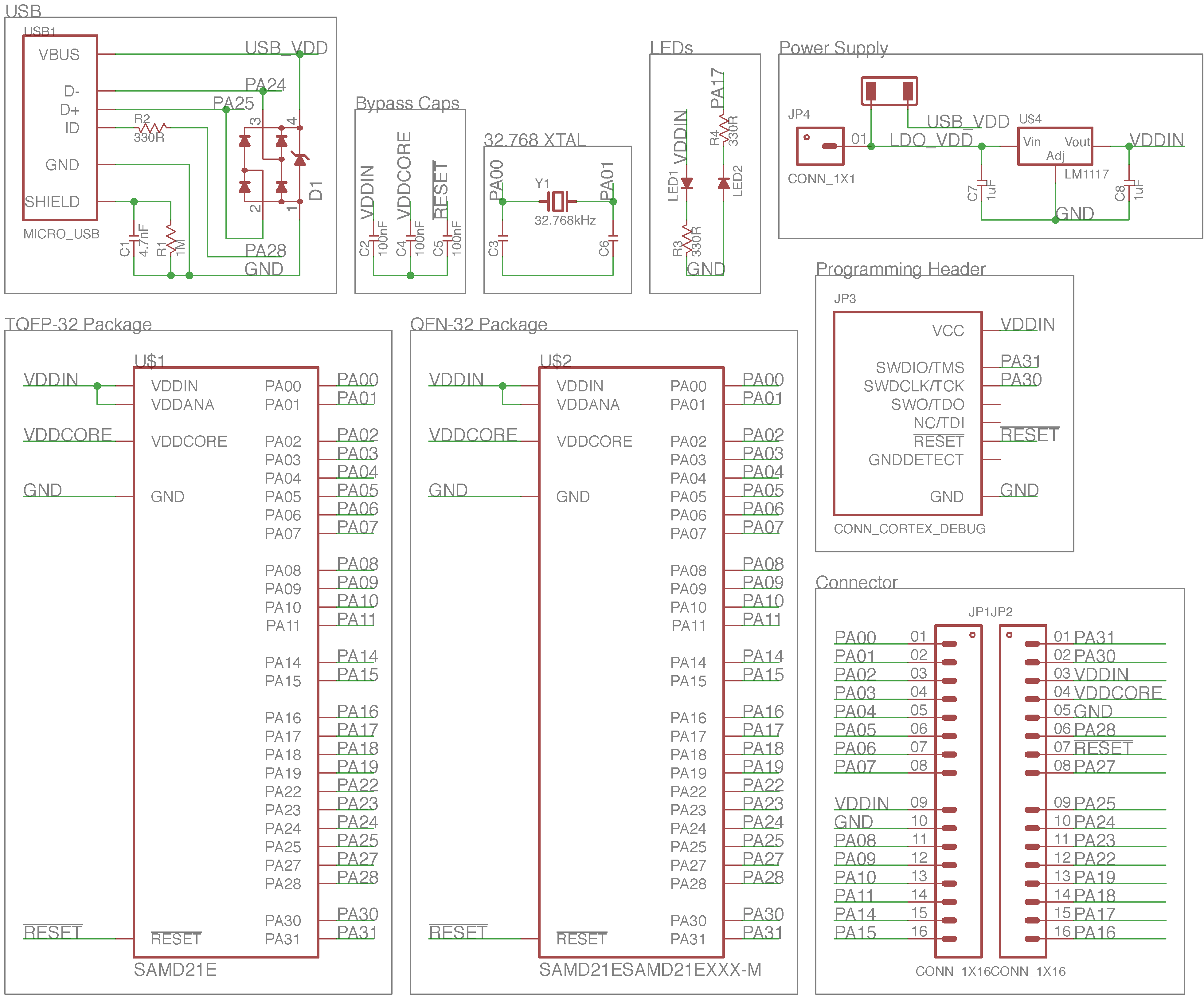
I've updated the schematics slightly prior to ordering the PCBs. This was done to reduce the board size further, which would enable me to fit substantially more on the panel I was ordering (the slight reduction in size meant the number increased from two per panel to five per panel).
The key differences (in order from Entry 1);
- The Chip Footprint has been replaced with both a TQFP-32 and QFN-32 package (so either package can be used on the breakout board)
- The symbol for the Programming Header has changed, as I wasn't happy with the library I was using for this part (I believe there was issues with the hole diameters on the footprint - I can't remember for sure though)
- The reset buttons have disappeared (there were two to allow either SMD or through hole buttons to be used, depending on sourcing). These were rather large, and personally I'm more inclined to add a reset button to the designs that utilise the breakout board if I feel it needs one, however for most of my designs a simple power-cycle is sufficient
- The 32.768kHz crystal was changed for a smaller SMD package, to reduce the size
- The USB ID pin now connects to PA28, rather than PA03
- And finally; the power pins have reduced from two to one, with a solder jumper (default: disconnected) allowing a connection between the USB 5V line and the power input pin. This means the board can still be powered from USB, but the removal of the protection diodes means care should be taken if soldering the jumper to power it from 5V, as this directly connects the Vin pin to the USB 5V rail.
Schematic below!

Discussions
Become a Hackaday.io Member
Create an account to leave a comment. Already have an account? Log In.