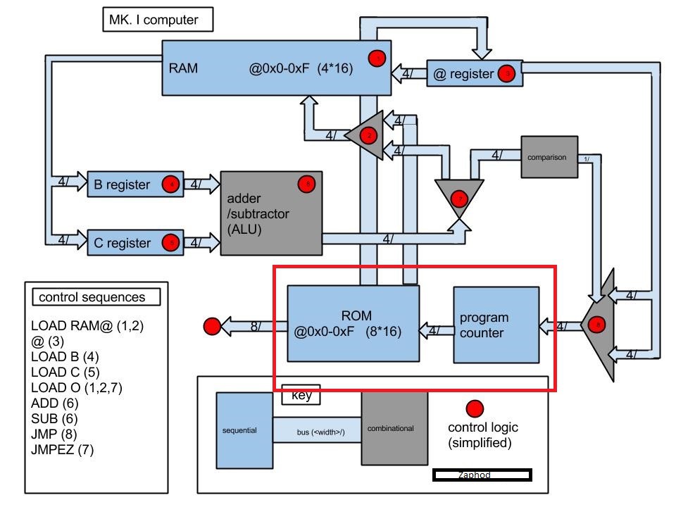
 zaphod
this is what I've been working on:
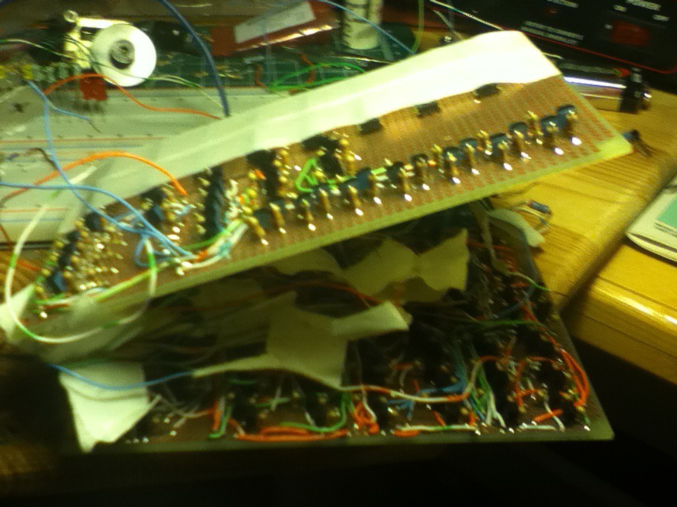
(I was once again unable to flip the photo)
for reference here's what you're looking at:
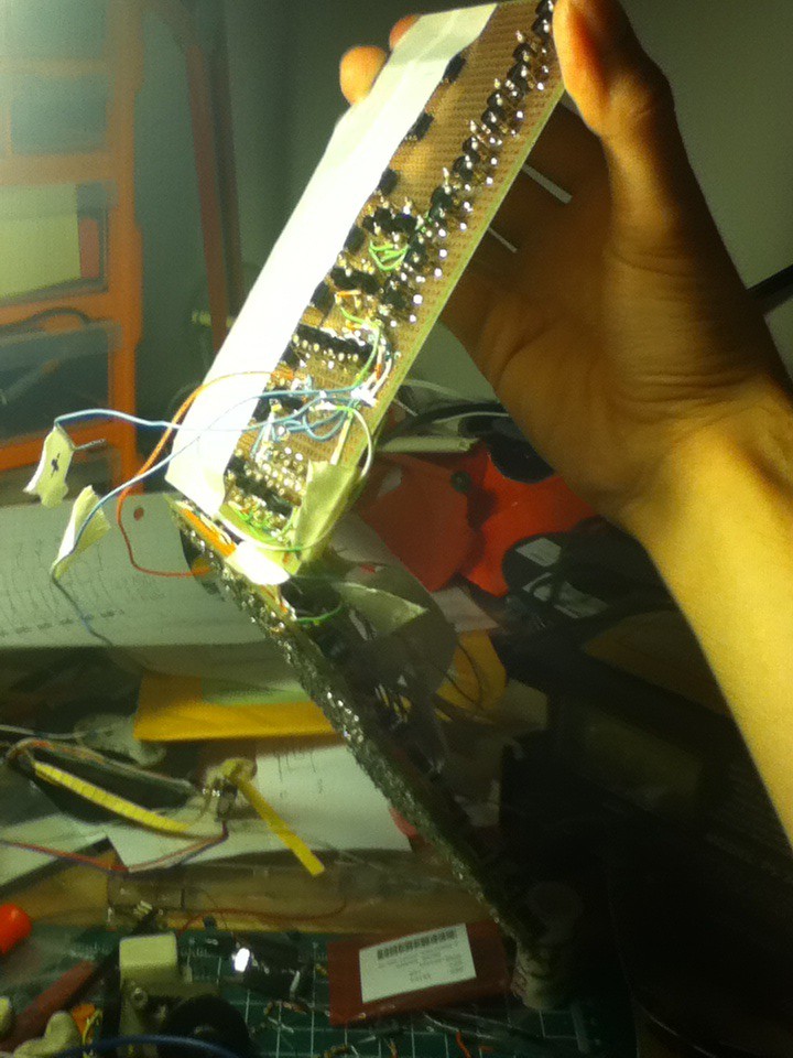
you may recognize the bottom board. it's most of the program counter. the top board is the extra logic that is necessary for the program counter, that I could not include on the bottom board. additionally the top board contains the beginnings of the ROM access logic. the stuff underneath the masking tape are the 16 DIP switches that will make up the ROM.
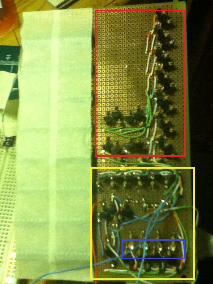
this is the top board. the stuff in the yellow box is the extra program counter logic. the blue box contains LEDs that will read out the memory address that the program counter is currently pointing to. the stuff in the red box is the beginnings of a multiplexer for memory access. this is the design I am using for the decoder half of the multiplexer:
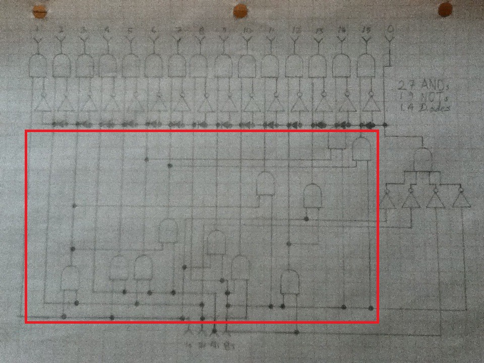
the red boxes correspond. basically what this circuit will do is translate a 4 bit binary number, say 0110 (6) into a single pulse on a 16 bit line, e.x.:
0110 becomes:
0000010000000000
and 1001 becomes:
0000000010000000
etc...
basically this circuit will allow a 4 bit number to select one memory address. the reason that the program counter counts in binary (0000, 0001, 0010, 0011, 0100, 0101...) rather than like this:
0000000000000000
1000000000000000
0100000000000000
0010000000000000
0001000000000000
0000100000000000
etc...
is because the program needs to be able to reset the program counter to a new memory address, however the computer can only process four bit numbers, so if the memory addresses were 16 bits wide loops would be impossible.
the next step is to build the remaining memory access logic.
Discussions
Become a Hackaday.io Member
Create an account to leave a comment. Already have an account? Log In.