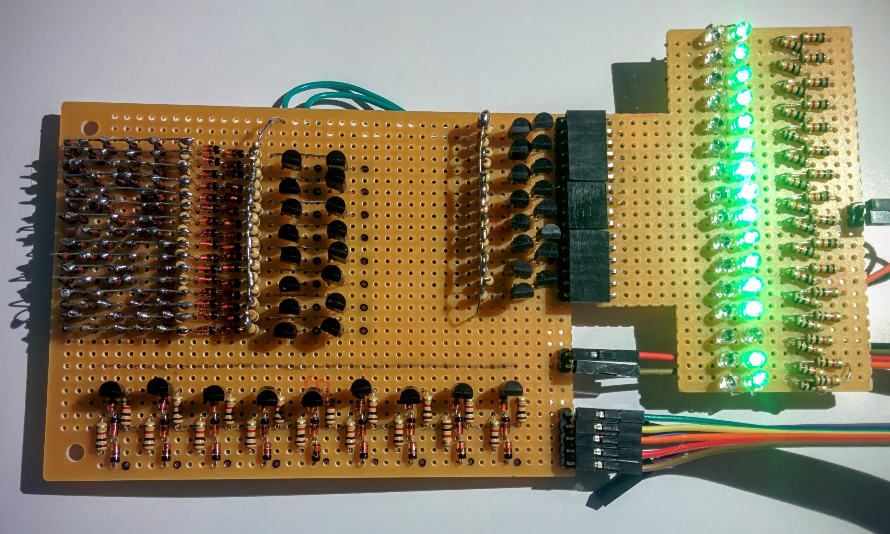
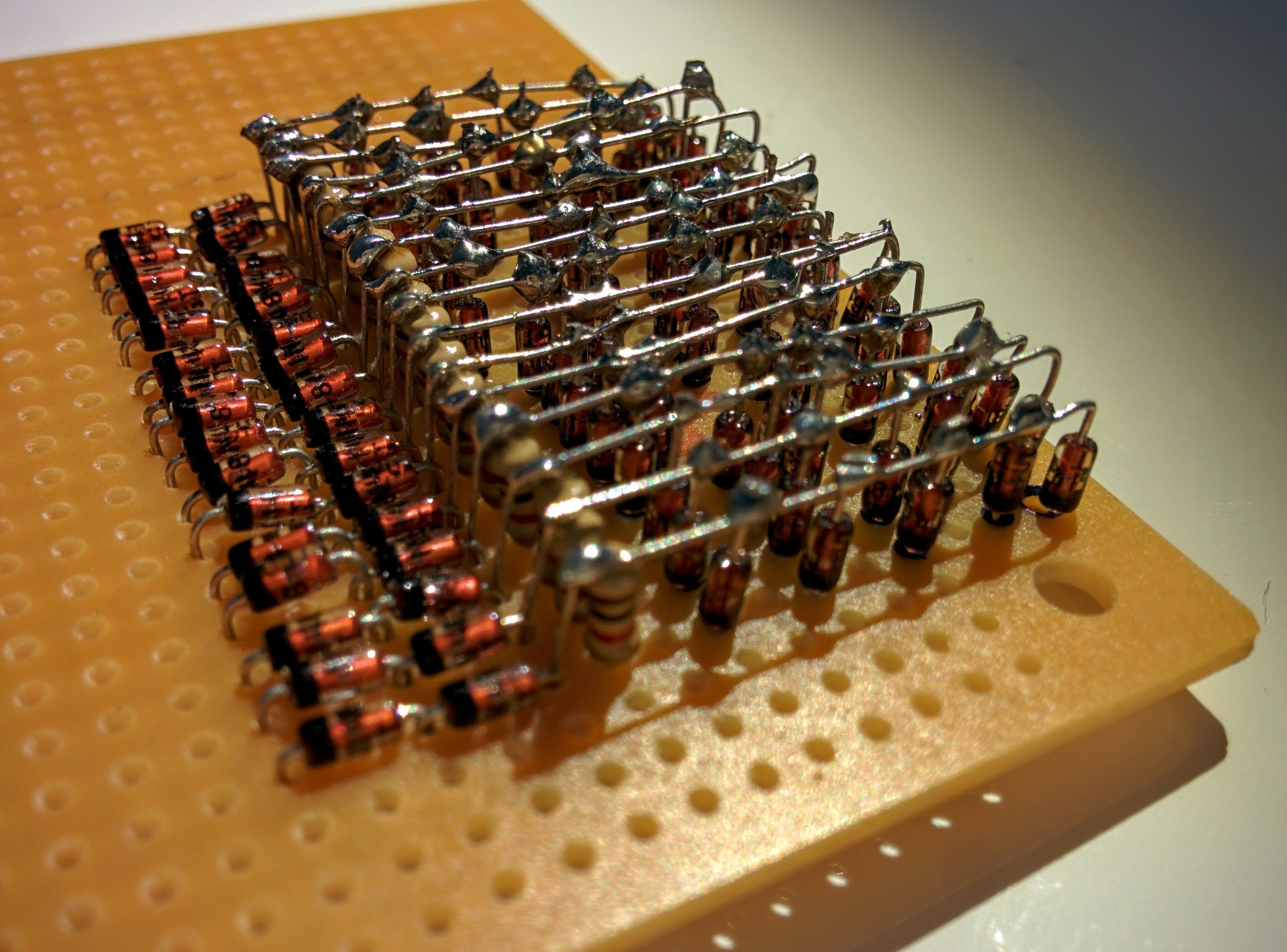
I've soldered up a 4-to-16 line decoder pcb. Two of those are required for the program address (ROM) bus, and at least two more for the data address bus (RAM).
I will have up to sixteen ROM boards each holding sixteen (11-bit) words of memory.
In order to not require local decoding of the last four address bits (A0..A3) on every ROM board I have a board like this that takes four binary bits and outputs one of sixteen select signals that goes out to a bus that all ROM boards are connected to. Then each ROM board will have a separate board-enable signal as well - or all boards would respond at the same time.
This decoder board is basically just five inverters (A0..A3 plus Enable) that is connected to sixteen 5-input NAND gates that are then followed by sixteen inverters that goes to the outputs of the board.
In total I ended up with 139 diodes, 50 resistors and 41 transistors if I've counted correctly.
I think I'll have to draw some block diagrams to explain the workings of all my pcbs and how they will be interconnected....


 matseng
Discussions
Become a Hackaday.io Member
Create an account to leave a comment. Already have an account? Log In.