A detailed documentation is of course necessary (and I'll write many notes here), but there are other things and features to add to the system, to make it more configurable.
First, make a better "internal bus" so any data (from the external SPI console or the onboard SPI memory) can be written to the Wiznet chip or the internal configuration registers.
Those registers control :
- RGB order: currently it's wired for RGB, but all other permutations are possible, GRB, GBR, RBG, BRG, BGR)
- number of channels (must be even)
- total number of LED [counted in pixels/2, or bytes/6]
- "Almost full" level of the internal FIFO [counted in pixels/2, or bytes/6], which must be LESS than the total number of pixels (Could be computed from the total number of LEDs but it's better to do it in SW, logic gates are precious) [to be verified, it seems i took care of that corner case already in the design)
I'll allocate addresses for these internal registers and the SPI flash will be able to configure them during the reset sequence.
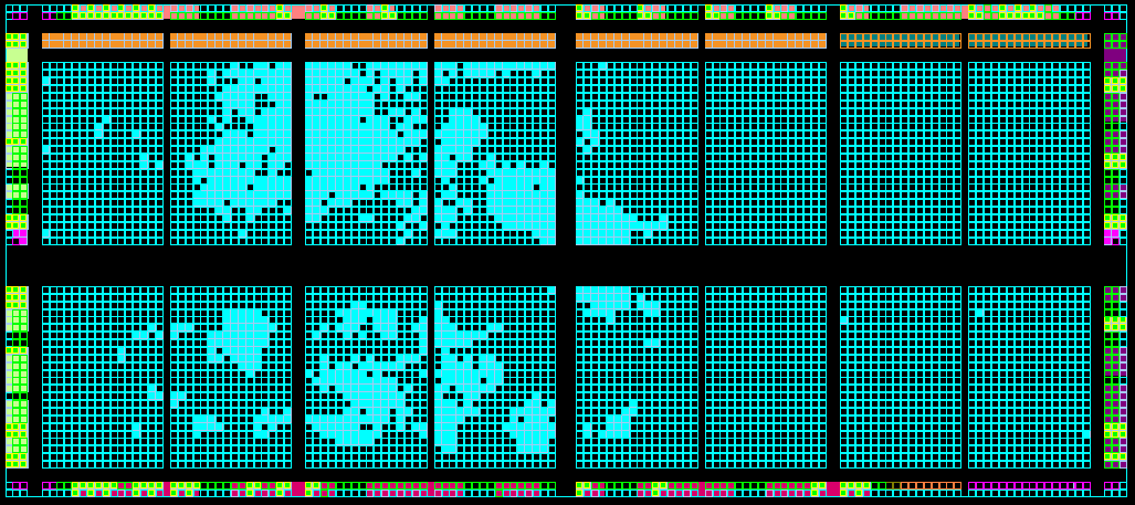
For a minimal configuration (8 channels implemented only) only 1/5 of the FPGA is used so there is some room for new features. Only 2 DP-SRAM blocks are left (1KB) though. The Actel chips are (most often) memory-bound...

It might be possible to store pictures in the onboard SPI Flash memory, that are displayed during the first seconds after startup, or when the network is down.
 Yann Guidon / YGDES
Discussions
Become a Hackaday.io Member
Create an account to leave a comment. Already have an account? Log In.