Kent
KentComponents:
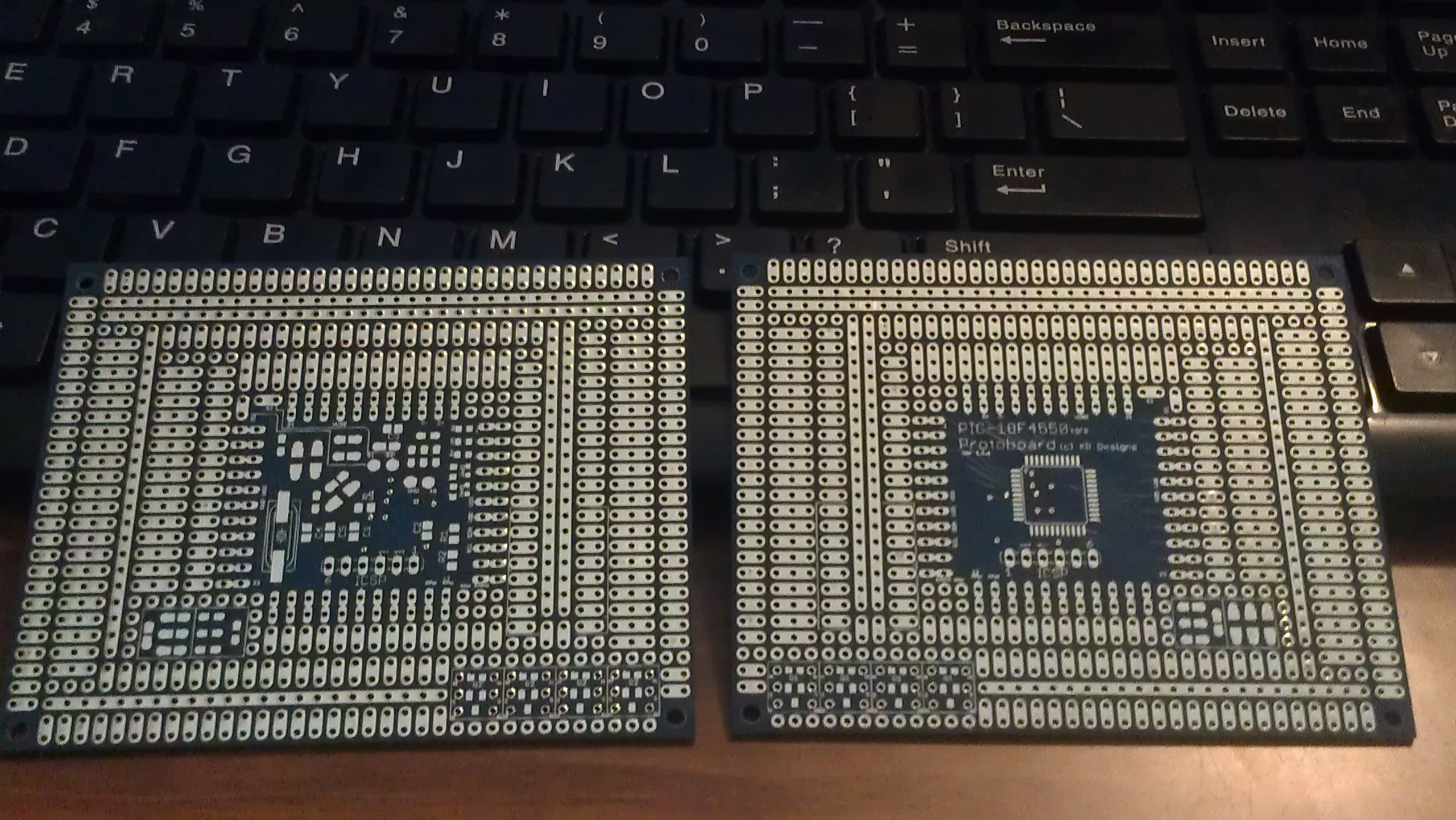
C1,C2 - Power caps (between VDD and VSS)
X1 - External oscillator
C4,C5 - Caps for external oscillator
R3 - ICSP Pull-up
R1,R2 - I2C Pullups (RB0, RB1)
C3 - Cap for Vusb
R4-6 - IO pin pullups (RD4, RD5, RC7)
led1,2 - 0603 led/resistor pair (RD6, RD7)
Some general notes:
I've mostly settled in on this PIC chip family for USB gizmos that need a 8-bit-lifting capacity. This layout was made with a few specific projects in mind that are likely to derive from a common hardware set. The design philosophy is based on using an I2C port expander to handle load switching (matched w/ transistors if desired) and reserving I/O pins for data exchange and analog sensors.
The TQFP package includes non-typical "Secondary ICPorts" that can be used for in-circuit debugging and programming - freeing all of the 4550's standard pins for IO while still allowing connection to a programmer/debugger. This board design provides an easy-access header for the NC pins.
The SOT23 pads are a double-sided design with breakout pins for Source, Drain and Gate. They're wired up for 2N7002 transistors - and should work with any transitor having the same package/pinout. I decided to save myself some wiring and drew a trace between the source pins of each package, which means that both transistors on a top-bottom pair will have to use the same voltage source.
Integrating SMD pads on the board is a complete experiment. The pads created integrate standard SMD footprints (0603,0805,1206) with a round wiring pad hopefully to allow jumping between smd devices or out to hole-through pins. The extra space on the bottom-side not needed for MCU accessories was used to make an experimental "SMD playground" with a handful of pads and two linked external break-out pins. Time will tell if any of that is useful.
Anyways. The fab apparently didn't choke on the gerber files ... so I guess we'll find out if this sucker works.