This primer walks you through the world of Hexabitz hardware. Keep in mind that physical realizations might change, but the core Hexabitz philosophy will always be governed by the following concepts.
1. Modularity is a Fundamental Concept
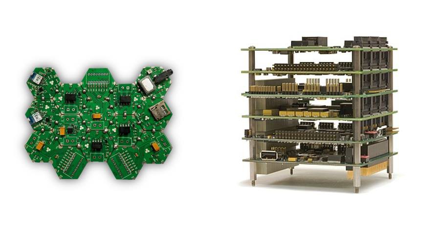
Hexabitz modules have basic modular geometric shapes (namely, hexagons, pentagons, squares and triangles) that wheb used with specific ratios, combine with each other to form contiguous surfaces. The modularity concept is found everywhere in nature from molecules and crystals to cellular and biological structures and even macro-structures (e.g., bee hives, insects). Why would you need a contiguous surface? Because it is more rigid, reliable and volume-efficient. It is also how most custom-made PCBAs are designed. And the ultimate goal of any prototyping/rapid-manufacturing platform is to mimic custom-made PCBAs as much as possible. Some geometric shapes even construct non-flat surfaces as shown below.
Modularity often translates into symmetricity, a very-tough design constraint. We strive to preserve modularity and symmetricity in all Hexabitz hardware and let these two characteristics guide design decisions. However, sometimes (not so often) we have to break the rules when it is near-impossible (or impractical) to follow them.

2. Form-factor is Important!
There is one basic shortcoming in many advanced electronics prototyping systems is that they are not optimized for form-factor, especially horizontal integration. This means they are not real-life-ready. Custom-made PCBs are horizontal by nature of PCB and semiconductor manufacturing techniques (traditional electroplating and lithography). By contrast, a configurable multi-module system that seeks access to same physical ports requires vertical integration. As a result, most prototyping solutions fail to produce a system that can replace custom-made PCBAs since they have a completely different form-factor.
Hexabitz emphasized horizontal integration from the beginning. This does not mean you can not do vertical integration. You can still mix both to create a complex form-factor. The only difference is that Hexabitz assembled boards (or arrays) are horizontal by nature. This makes them perfect substitute for custom-made PCBAs.
Form-factor has another dimensions to it, including volume and weight. Hexabitz mainstream implementation seeks to optimize weight and volume (and cost) as much as possible and thus eliminates connectors, wires and attachment mechanisms in favor of a simple and effective solder-based, exposed-PCB-edge connector system. Other implementations might optimize for different variables and offer different solutions.'

3. Dual-end System for Flexibility and Scalability
In order to build a truly scalable solution, one that works for virtually all types of functionality and for arbitrary number of modules, Hexabitz is based on dual-end module architecture. The front-end is the module part (hardware and software) responsible about its unique functionality. The back-end is the module part handling all background activities including communication, addressing and other array-related functionality. The back-end, often represented by the MCU on module bottom side and the Bitz Operating System (BOS), effectively virtualizes and standardizes the interface to any type of front-end, whether it is analog signals, high-power motor, high-speed FPGA or just plain bits and pixels, they all share same interface to the Hexabitz ecosystem. The back-end resembles infrastructure in computer and communication networks, necessary to scale and standardize but not beneficial on its own. The front-end is the useful part of the process providing the end application.
The dual-end system necessitates using an MCU in every configurable module (i.e., one that can change any of its parameters as opposed to a dump battery module for example.) One might worry about cost or power consumption. The mainstream Hexabitz implementation is built around ARM Cortex-M0 MCUs, the industry-leading devices in efficiency and low-power consumption. These tiny beasts, if optimized well, are powerful enough to carry on all of the back-end (and some front-end) tasks while leaving minimal cost, weight and power consumption overhead. The massive gains in configurability and true parallel execution dwarf any overhead.
Module Anatomy
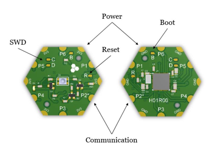
A typical configurable module (i.e., one that has an MCU) is shown in Figure 3. The top side (left) features front-end components (in this case an RGB LED) and the bottom side features the back-end hardware (i.e., the MCU).
Exposed copper areas on module corners and sides are used for physical and electrical connectivity in Hexabitz mainstream implementation. Corners are always used for power (+3.3V on top and 0V/Ground on bottom) while sides are always used for communication (TXD/transmission on top and RXD/reception on bottom). Communication ports are numbered sequentially (clockwise) starting from P1 in the module upper right corner. Some modules do not have the full set of power and communication ports due to space constraints or conflicts with other connectors. Communication ports allow serial communication (UART) between modules as well as connect the modules to the external world (e.g., cables, other boards or electronic devices). These ports can be re-purposed in many modules for other functionality (e.g., connecting input switches or different communication interfaces). Bootloader-based firmware update is also possible through communication ports. The port marked with (*) can be used with ST factory bootloader in the mainstream implementation, i.e., it allows firmware upload to an empty MCU. All Hexabitz modules back-end circuitry operates on 3.3V from the power ports. Voltages higher than 3.5V should never be applied to power or communication ports!
Another set of exposed, non-edge, copper areas (or pads) are used for non-essential connections such as programming/debugging. The MCU serial-wire debug (SWD) interface can be accessed through pads C (clock) and D (data) for programming and debugging. MCU reset pin is available on pad R and boot pin on pad B. These pads are duplicated on both module sides to allow surface connection to either side (or even though-hole connection by drilling the pad). Different Hexabitz implementations might have different set and characteristics of exposed pads.
Almost each Hexabitz module has at least one indicator LED on module top side. The general indicator LED for all modules is red-colored. It is useful to debug module status and relay various visual messages to the user. Some modules have extra indicator LEDs with different colors to convey other states (e.g., input or output power, communication, etc.)

Module bottom side features, almost always, module part number while the top side has Hexabitz truncated logo on the silkscreen. Never the less, it is recommended to distinguish sides using power connectors. Top side will always have the positive voltage (~3.3V) while bottom side will always have the ground (GND).
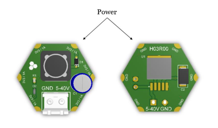
Figure 4 shows a non-configurable module. This one provides power to the array and thus features only power ports. Note that some power modules are designed to generate output voltage a bit different from 3.3V (e.g., 3V) . They can still power other modules but with possibly some functionality limitation.

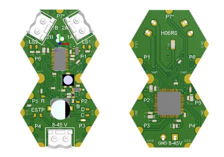
Some modules might have mounting holes but it is not generally the case with most of them. Another special case happens when there is not enough real-state to fit the module front-end functionality (figure 5), the module will then grow in size by permanently stacking multiple geometric shapes (e.g., two stacked hexagons). This ensures the module still adheres to modularity principle and geometrical properties of Hexabitz arrays and thus can interface easily with any other modules.

The Array
When Hexabitz modules connect to each other, they form arrays. Arrays can have contiguous modules or ones that are kilometers away. They can be flat or curved, horizontally integrated or have a complex 3D form-factor. In theory, there is no limitation to number of modules in an array. In practice, physical limitations such as power drop and MCU memory size make it difficult to build arrays with very large number of modules. It is still possible, however, to connect as many as 100 modules together without any special interfaces. Much more than you can connect with many other platforms and in a much smaller form-factor.
Hexabitz arrays are pure peer-to-peer, mesh networks. We abandoned the conventional solution of a bus-architecture to remove any constraints related to bus topology or capacity. Hexabitz modules can connect to each other using any communication port to form any physically-possible configuration. The only assembly constraint is to make sure contiguous modules have same orientation (i.e., all facing up or down) to avoid shorting power.
Arrays are also fully distributed and decentralized systems. There is no requirement for a router or switch or main controller and thus no point of failure. The array could function in a completely decentralized way, or act as slave devices for a master module or an external controller. All depending on firmware implementation. Eventually, we hope that most of behind-the-scene work to facilitate this architecture will be carried out by the BOS to free users to focus on the end-application. All configurable Hexabitz modules are valid entry points into the array and are able to receive user commands (e.g., through BOS messages or the Command Line Interface-CLI) and process locally or forward to destination module(s).
One might be worried about latency in a peer-to-peer architecture. It is a valid concern. However, in practice, about 90% of typical applications will not suffer any latency limitation. First of all, inter-module communication is based on an optimized mix of high-speed hardware UART peripherals and direct memory access (DMA) channels. The combination of these two technologies offers a streamlined way of transferring data across the array without requiring much CPU intervention. As a result, modules can bypass communication messages with virtually no delay or CPU down-time. Hexabitz mainstream implementation can stream data across the array in speeds that can reach 1 Mbps or higher in specific configurations. Although the number might seem low for streaming applications, it is a relatively high datarate for control networks, which brings us to the next point in this discussion: Hexabitz back-end is optimized to stream control messages and not for bulk data transfers. By definition, a bunch of in-homogeneous modules (e.g., an LED, a motor drive, a BLE radio and a temperature sensor) have few things in common and will mostly need to exchange control messages occasionally. Bulk data transfers can be facilitated with other methods that break the modularity principle. Given said that, the mainstream implementation is not the only possible way to work with Hexabitz as explained in the next section. One can envision a custom implementation utilizing much faster MCUs (and even FPGAs) in the back-end if the application calls for this requirement.
Custom Implementations
Hexabitz is based on the assumption that custom electronics will always be more expensive for low quantities, take more time to make and serve only a single purpose. Although the concept itself is flexible enough to cover so many applications, one still need to make few customized decisions regarding physical implementation. I designed Hexabitz mainstream implementation to cover the requirements of majority of anticipated real-life applications. These requirements include among others:
- Full flexibility and upgradability.
- Optimized form-factor (volume and weight) to mimic custom PCBs as much as possible.
- Cost competitive solution to enable low-volume production.
- A compromise between array stiffness / reliability and assembly time.
- Robustness and reusability rate of at least 10 times during product lifetime.
Some applications, by nature, have different requirements. For example, a K12-kid-friendly application will need to replace soldering with plug-n-play connectors; a delay-intolerant application might require much faster (and more expensive) hardware for the back-end; and a safety-critical application will require even different types of components all together. Some customization might preserve components but use different solder mask color or larger (or smaller) module size or even replace the PCB with an FPC (flexible printed circuit). Still, they can all preserve same basic principles listed above. Initially, we will not target these special implementations and will focus only on the mainstream implementation (unless you have enough budget to pay for a custom set!). As time progresses, however, scale economics and network effects will make it economically feasible to offer more customized implementations.
 Hexabitz
Discussions
Become a Hackaday.io Member
Create an account to leave a comment. Already have an account? Log In.