 Yann Guidon / YGDES
The Winbond 25Q128 is a really cool part : high capacity (16 MBytes), very fast, good support for many standard instructions, supports wide bus modes... But it can be expensive depending on the application.
I found the little sister 25Q32 : I use 6 of them on each board of a project. I expect it to be almost exactly the same as the 25Q128 but with only 4MBytes (so the board has 24MB, still nice). I got them off eBay and received them. Now comes the time to try them !
As I am writing a detailed tutorial, I want to use this project log to show how to add a part to the SPI flasher so others can add their own (and as much as possible provide feedback so I can make this system better, for me and everybody else).
First, let's get the datasheet !
Google gives the right PDF on the first result when I type "datasheet 25q32bvsig". The file is on the Winbond website and I miror it on my own site http://ygdes.com/pdf/Flash/, for archival and easy retrieval.
Let's analyse the data :
- The device operates on a single 2.7V to 3.6V power supply : 3.3V compatible voltage : check
- Standard pinout : check
- 256-byte per programmable page : Page Program instruction (02h) accepts up to 256 bytes : check
- Clock frequency for Read Data instruction (03h) 50 MHz max : check
- Uniform Sector/Block Erase (4/32/64K-bytes) : Page Erase instruction SE (0xD8) erases one 64KB block : check
- nothing sounds unusual...
More analysis is necessary to complete the description and table in SPI_Flash_chips.h but it seems to follow the 25Q128's definitions so this is just a matter of checking that every instruction matches.
The 25Q32 follows all the conventions so it's safe and easy to use with the flasher. I can update SPI_Flash_chips.h :-)
Let's now solder !
I also bought some tiny DIP8-SOIC8 adapter boards on eBay so I can test them in the common DIP8 socket. I have a SOIC ZIF somewhere but it's not very practical. The PCBs need pins too: these come from special DIP8 sockets that I hacked a bit and provides a sturdy base, but you'll use your own parts.
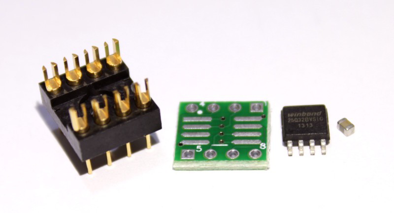
This time I put the capacitor directly close to the chip's power supply pins.

Now I can test it !
I power the Raspberry Pi on, looking at the HDMI screen that displays the boot logs.
My IP address is 192.168.41.100

pi login: _
I see that Apache is working when I browse to http://192.168.41.100/ and I access the YGWM interface. I can now login through ssh:[yg@localhost ~]$ ssh pi@192.168.41.100 pi@192.168.41.100's password: pi Linux pi 3.12.28+ #709 PREEMPT Mon Sep 8 15:28:00 BST 2014 armv6l /dev/root on / type ext4 (ro,noatime,errors=remount-ro,data=ordered) remount RW pi@pi ~ $ _This Pi boots in "read only mode" so you can turn it on and off without concern of filesystem corruption.
The software tools are installed in the Apache data directory. I go there to execute one of the test programs:
pi@pi /var/www/C $ sudo ./test_SPI_Flash

SPI Flash Signature :
 EF 40 16 00 00 00 00 00
 15 15 15 15 15 15 15 15
Status Register = 00
 * Ready
 * Write disabled
 * Array is unprotected
{
  start=0,
  data=[
83,0,41,29,133,3,64,18,0,12,127,0,125,0,123,128,
18,0,8,126,0,127,4,125,255,18,0,10,144,255,0,224,
...
1,184,0,0,0,0,0,2,1,191,67,111,112,121,114,105,
103,104,116,32,49,57,57,57,45,50,48,49,48,44,32,97 ]
}

Setting pins 8 9 10 11 22 as input
It dumps the 256 first bytes of the Flash array into a JSON string and it is surprisingly not empty.I can now copy the extracted signature (very similar to the 25Q128) and paste into the chips library :
pi@pi /var/www/C/src $ nano SPI_Flash_chips.h

                      0xD8   0x03            Bulk
                     Sector   Page  Freq     Erase    Test            Signature
               Mbits  Erase  write  (MHz) (s)  (DS)   R/W     RDID            RES
25LC1024        1     32KB    256     10   0?  (2-4)   OK    (0)+            (29)+
M25P40          4     64KB    256     75   5 (4.5-10)  OK   20 20 13 (00)+   (12h)+
A25L40P         4     64KB+   256     85   2  (6,12)   OK   (7F 37 20 13)+   (12h)+
SST25VF016B    16     64KB      x     50               KO   (BF 25 41)+      (BF 41)+
SST25VF032B    32     64KB      1     80               1o   (BF 25 4A)+      (BF 4A)+
AT26DF321      32     64KB    256     66  39           OK   1F 47 (00)+      (00)+  (sold protected)
W25Q32B        32     64KB    256    104   5 (7-15)    OK   EF 40 16 (00)+   (15)+
W25Q128F      128     64KB    256    104  40 (40-200)  OK   EF 40 18 (00)+   (17)+
There are other parameters to report, such as the chip erase time (it's not critical but good to know). The command is shown below:pi@pi /var/www/C $ time sudo ./wipe_SPI_Flash
Status Register = 00
* Ready
* Write disabled
* Array is unprotected
4s /
Setting pins 8 9 10 11 22 as input
real 0m5.070s
user 0m0.030s
sys 0m0.020s
pi@pi /var/www/C $ _5 seconds is less than the 7 to 15 seconds of tCE in the datasheet but it's normal for a brand new chip. A deeper reading of the datasheet lets me complete the instruction table, which is not as extensive as the 25Q128 but comparable to the other 32Mb parts.
Finally, I access the #YGWM interface to edit codes and when I click on the "Flash .HYX" button, the chip is correctly overwritten and updated by update_SPI_Flash.cgi. Success !
Discussions
Become a Hackaday.io Member
Create an account to leave a comment. Already have an account? Log In.