 Yann Guidon / YGDES
This log updates/replaces "Board 2 : Register set".
See the update at "The registers"
The YASEP has 4 types of registers in the register set.
Except the "Data" registers, which are mapped to the memory banks' ports, the registers can be incremented or decremented as part of most opcodes.
The PC is a bit special because it is incremented automatically, so post-updates should not have any effect. But PC, Rx and Ax are 11 registers that are implemented as up-down counters in this project.
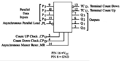
The 16-bits counters are made of 4×74HC193, preloadable 4-bits up-down counters. That's already 44 chips...
One nice unexpected advantage is the ability to clear/reset the counter at will, which is not a feature found in modern register sets. This could be useful for debug or clean startup.
The two read ports need their set of chips that send data over their respective buses. The initial version used a bunch of 74HC594 but they don't provide inc/decrementation. Using a counter requires the use of simple buffers like the 74HC245.
However this creates layout density problems. Another problem is the capacitive load on the bus, with more than 16 drivers that turn into loads when off.
The solution is the 74HC253. It's a double MUX4 with tristate output and common address.
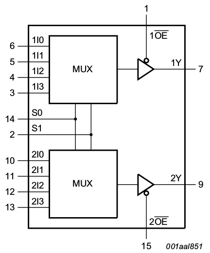
Iit's perfect for the situation because it reduces by 4 the number of pins on the buses. In fact it actually reduces the overall number of pins so the required PCB surface is a bit smaller. Here is the rationale:
- With the '245 method, for one register, the 16 output pins of the '193s go to 4×'245. The output pins of these '245 share the same signal as the 4 other registers so the '245 have a total of 16×5 separate input pins but 16×5 shared outputs
- With the MUX4 method, there are 5×16 bits input pins but only 16 output pins so 16×4 pins are saved.
(of course the calculation does not work this well because of overhead with the smaller DIP package and the additional '157, see below)
The '253 also forces bits to be spread out and this reduces the routing bottleneck.
One 16-bits read bus requires 8 such ICs.
- Memory bank 1 can select between A2, D2, A3, D3.
- Memory bank 2 can select between A4, D4, A5, D5.
- Program Memory board can select between PC, A1, D1.
(...)
It seems yes, easily:
- P2 : Registers : R2, R3, R4, R5 (2, 3, 4, 5)
- P3 : Program Memory : PC, R1, A1, D1 (0, 1, 6, 7)
- P4 : Memory bank 1 : A2, D2, A3, D3. (8, 9, 10, 11)
- P5 : Memory bank 2 : A4, D4, A5, D5 (12, 13, 14, 15)
Overall, the loads on the read buses will be one HC gate per board (front panel, register set, 3 mem boards, ALU). 6 loads is reasonable so the running speed can be a bit better than I expected... But there will be 64×'253 to wire !
Discussions
Become a Hackaday.io Member
Create an account to leave a comment. Already have an account? Log In.