 Yann Guidon / YGDES
(Obsolete but interesting anyway)
The second board is the simplest and the illustration of many of the principles of this project.
Here is a more-or-less 1:1 scale layout :
It's "simply" a bunch (20) of 74HC573 8-bits D-FlipFlops.
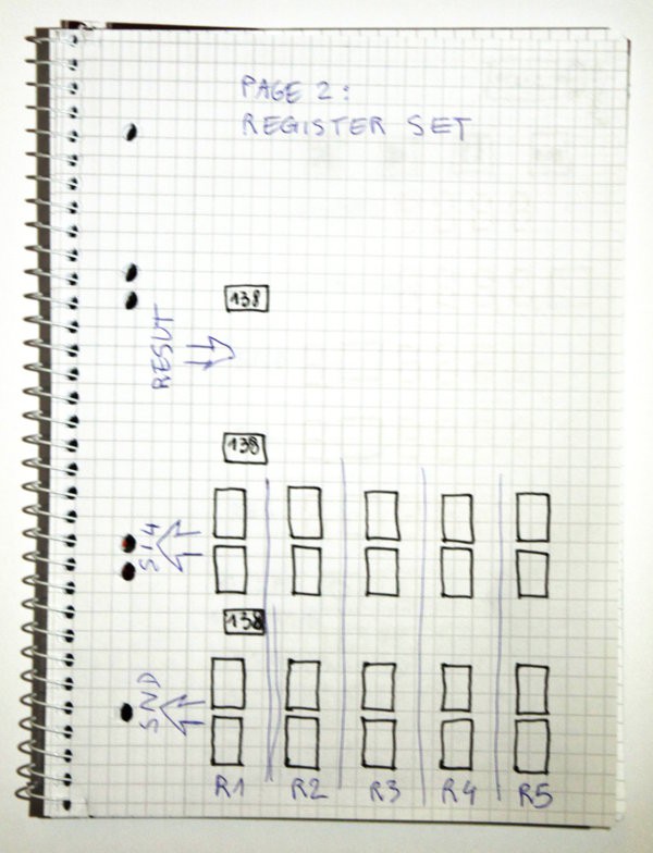
In the YASEP architecture, registers R1 to R5 are "simple", just like in most RISC designs. They have no side effect : they can be read and overwritten like any memory cell.
They are "materialised" by these 8-bits SOIC chips and provide a physical sense of where data reside.
Each register is 16-bits wide so 2 SOIC chips are required per read bus.
There are 2 read busses (SI4 and SND) so the chips are duplicated (the data are stored redundantly). This is actually a compromise to reduce chip count. Each SOIC chip will drive its read bus only when selected, its output remains in high impedance otherwise. Other methods of 2reads-1write would instead use 1 DFF chip and 2 multiplexing chip (either a 8->1 MUX or a 74HC245).
A normal MUX is the preferred method for high-speed designs but the YASEP's register set is not homogenous and it would make the board too complex.
Three 74HC138 select one of the 5 registers for read and write. Outputs 0, 6 and 7 are left open on this board but other boards (memory) use them.
Discussions
Become a Hackaday.io Member
Create an account to leave a comment. Already have an account? Log In.