-
Bare 486 and 8-bit "memories"
11/09/2015 at 09:57 • 10 comments(If anyone wants to host the 24MB PDF datasheet, lemme know! Apparently google-sites doesn't handle files that large(?!). I OCRed it, albiet not very well... but it's at least searchable, now...)
So, it would seem, random unreliabilities on boot was (mostly) due to a very important but overlooked fact:
Despite the ability to interface directly with 8-bit devices*, the 486 expects to read those bytes one-by-one on the 4-byte data-bus, aligned as such**:ByteAddress%4 Data Bits 0 D7-0 1 D15-8 2 D23-16 3 D31-24
*Section 10.1.1.1: "The Intel486 processor includes bus control pins, BS16# and BS8#, which allow direct connection to 16- and 8-bit memories and I/O devices"(Hah! "Direct" my a$$!!)
**Table 10-4. "Data Pins Read with Different Bus Sizes"
(This has been cut-down to only show 8-bit transactions with one ByteEnable active):BE3# BE2# BE1# BE0# with BS8# 1 1 1 0 D7-D0 1 1 0 1 D15-D8 1 0 1 1 D23-D16 0 1 1 1 D31-D24
Actually, if I understand correctly, each transaction *starts* as a 32-bit transaction.
(Unless, maybe the instruction itself is accessing only 8 or 16 (or even 24!) bits of memory.)
Then, the device (or chipset) immediately responds with an indication of the bus-size (if smaller than 32-bits), at which point the processor only reads the bits that would be valid in such a case, then will request the next byte(s) as necessary. So, e.g. if it's looking for 32-bit data (aligned at Address%4==0), it'll first send ALL ByteEnables active: BE3#-BE0# = 0. It will ask for all 32 bits it's looking for. Then the 8-bit device will tell it "sorry, I'm only giving you the first byte", and it'll read that one, then request the second byte, and so-on.
So, technically, each transaction is started with no knowledge of the device's bus-width.
(And, oddly, the datasheet actually mentions the odd-case where, say, a device might actually switch the number of data-bits it can supply in the middle of a (32-bit or less) non-burst transaction. Weird?)
Anyways, the end-result is thus: I had already wired D7-D0 for NOP (10010000) via pull-up and pull-down resistors, before I discovered the above, later in the manual... So, now, I had to wire-up D31-D8, as well, each byte with a NOP. At first I was planning to use pull-resistors as with the first byte... but after much procrastination it occurred to me *why* I was procrastinating: What if I want to change the instruction later down the road...? Yahknow, maybe eventually hook up an actual memory-device (ROM? again CRAZY!)... Simple Solution: Instead of pulling the remaining bytes straight to VCC or VSS, instead pull them to D7-D0.
And then... that's still a LOT of resistors... so had another crazy idea, resistor-networks.![]() I used straight-through DIPs, and bent the pins straight out the packages...
I used straight-through DIPs, and bent the pins straight out the packages...
So, now, each bit in each of the four bytes basically looks (roughly) like:
      V+
       ^
       |
       /
       \  10k
       /
       |
D7 ----+------.
       470    |
D15 ---/\/\---+
       470    |
D23 ---/\/\---+
       470    |
D31 ---/\/\---'
(Values were chosen somewhat arbitrarily based on what I had laying 'round...)
Or:D6 ===========+====. 470 | | D14 ---/\/\---+ / 470 | \ 10k D22 ---/\/\---+ / 470 | | D30 ---/\/\---' V GND
There're a couple cases where the resistor-networks were so long they impeded upon other surrounding pins, including in some cases a bit on the first byte, so we have, in those cases, something like:
       ^
       |
       /
       \  10k
       /
       |   470
D7 ----+---/\/\---.
           470    |
D15 -------/\/\---+
           470    |
D23 -------/\/\---+
           470    |
D31 -------/\/\---'
So, it was a bit of a crapshoot whether the loading of all those pins would interfere with the read-values, but it seems alright.
So, at this point:
It seems to "boot" reliably... As long as I let the power completely drop to 0V when switching off, before switching back on. (Hey! Maybe I don't need a schmitt-trigger nor D-FF on my reset after all! Nor gating on the clock! Awesome! Though, 24 resistors was a bit annoying...).
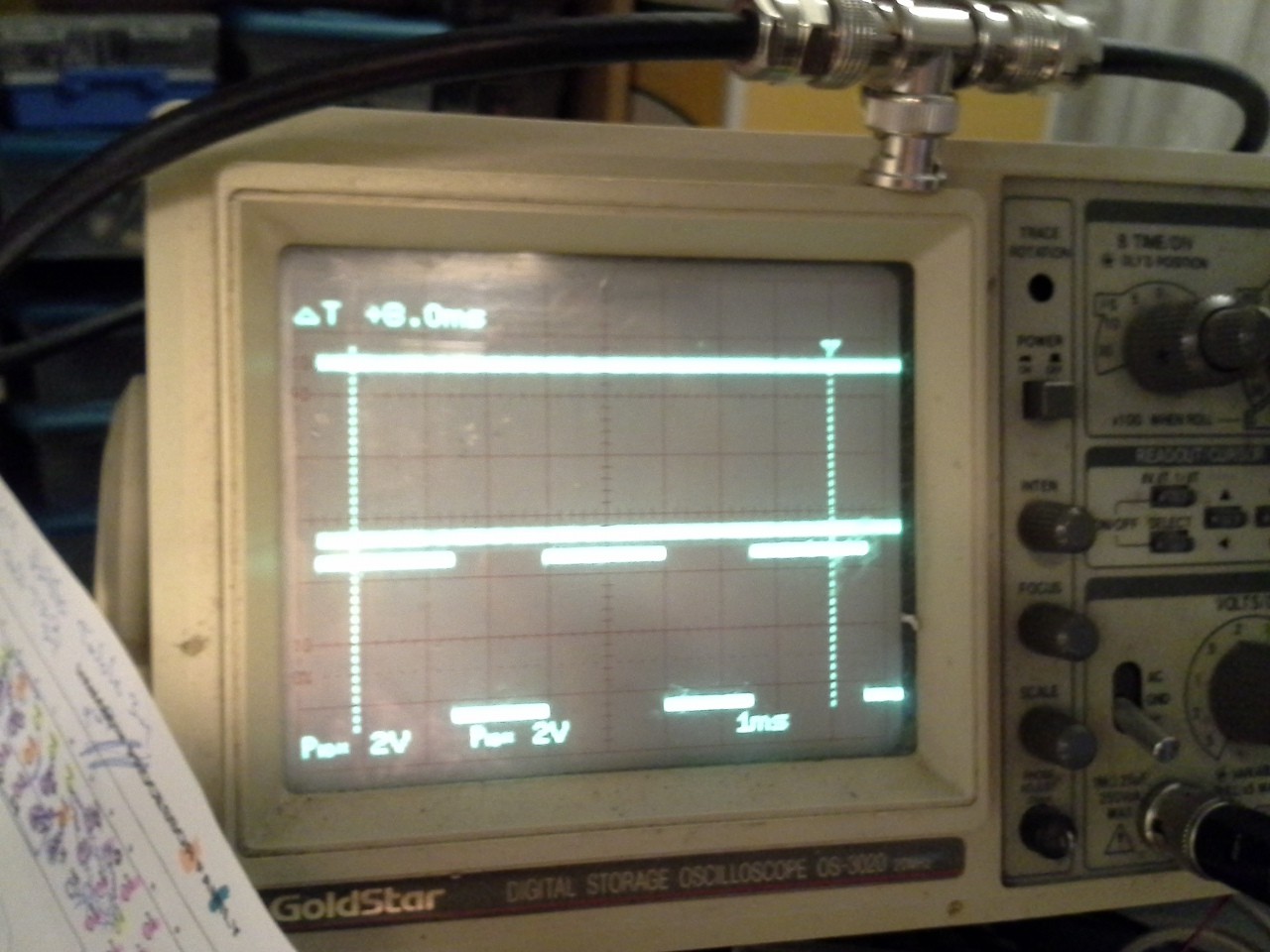
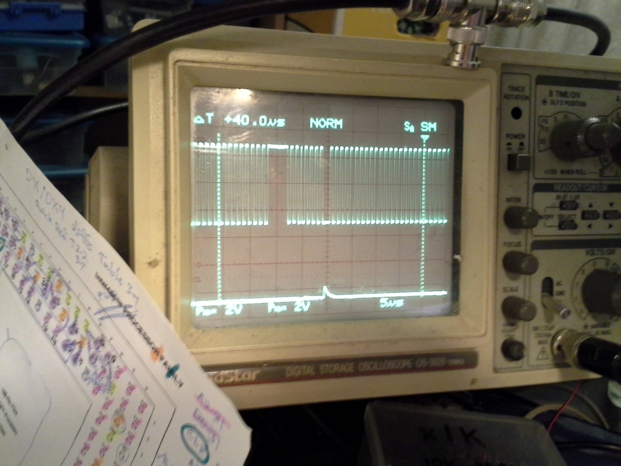
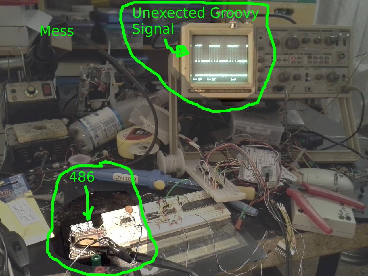
Its functionality seems pretty consistent; it seems to cycle through addresses as expected. But there are some remaining oddities. Didn't bother to check A27 first, this time, as I did last time, since I'd read somewhere that upon reset it only accesses the first 1MB, then wraps(?). But I did check A17, which should be in that 1MB realm... and Nada. Went down from there and noticed A14 isn't square:![]()
Then A12 is even weirder:![]()
And, sure-enough the processor is still driving the data-bus at some point or another...![]()
So, this "project" doesn't really have a particular direction... as it is, this is kinda cool.- I could start experimenting with really low speed clocks... (Was thinking about maybe making an arbitrary-clock-generator, maybe via PIC or AVR? Could be a useful tool to have 'round)
- I could look into the non-1MB wraparound issue (Likely will lead into figuring out why the processor is taking the data-bus... Probably will lead into learning a lot more about the architecture)
- Could look into delaying the "Data Ready" signal, e.g. for pushbutton-stepping, and-or slowing the "counter" (address-incrementing) via an R/C-delay
- Surely more, but I'm drawing a blank at the moment...
But I could definitely do with some blinking, soon!!! -
bare 486 chip oddities and misunderstandings...
11/08/2015 at 13:07 • 0 commentsI was just reading about the Byte-Enable pins (BE3:0) and how to convert them to A0 and A1. (Note the address-bus doesn't actually output A1 and A0, it starts at A2!)
Took a few minutes to wrap my head around it, but soon thereafter it seemed intuitive if not cut-and-dried to me: each byte-enable represents a value on A0 and A1...
A1:0   BE3  BE2  BE1  BE0
0      0    0    0    1
1      0    0    1    0
2      0    1    0    0
3      1    0    0    0

(actually, BEn are active-low,
 but this is easier to visualize)
BUT NO!!!!
Since it's designed for 32, 16, and 8-bit devices, there are cases where multiple BEs are active at the same time... somehow that hadn't occurred to me. So decoding is a bit more complex than I thought.I'm staring at a table in the datasheet as we speak, and my brain's just not parsing it at the moment...
And then, on top of that, there's a new oddity I just discovered, the datasheet says the 386 used to expect all 8-bit reads/writes on D0-D7... This is what I'd expect, seeing as how an 8-bit device only has 8 data lines, where else would one wire them besides the first 8-bit data-lines of the processor...?
BUT the 486 actually reads different data-pins depending on which byte it's reading, even when reading an 8 (or 16) bit device! So even if an 8-bit device is connected, and even if it's indicated with /BS8, it has to have its 8-bits repeated on (or rerouted to) each byte of the data-bus: D0-7, D8-15, D16-23, and D24-31. WTF. Apparently the chipset usually handles fanning it out like that.
"The external system must contain buffers to enable the 486 to read and write data on the appropriate data bus pins" LOL.
OK, so, for my NOP experiment that basically means I have to wire up all 32 data bits, so I guess there's no particular reason to use /BS8 (except maybe to intentionally slow it down... hmm).
So this *definitely* would cause issues with the instructions actually being read as NOPs... I've got floating inputs!
That's not to say there aren't other reasons for oddities, so @Nicholas Amrich, and others, keep those ideas coming, and thanks!
There are a couple other things I hadn't considered in my *really simple* circuit...
The CLK signal is supposed to be applied only after the power is stable... This one is, plausibly, a bit unlikely to cause difficulties... the datasheet says something like "Prior to this datasheet, this was unspecified, so this is *best-practice* that will be guaranteed to work now and in future versions of x86 processors..." ish. So, realistically, it's entirely plausible most motherboards supply the clock as soon as it starts oscillating, just as I have.
And the reset thing, did I mention that before...? I think it would be wise to feed that through a shmitt-trigger and possibly a D-Flip-Flop...
-----------------
This is getting a bit more complicated than I intended... Really, I just wanted to see what I could do with the simplest circuitry possible (a clock and a few passives was all I'd intended. Notice it's dead-bugged!)
But, I am learning some stuff I never expected to, and it's kinda interesting, and some of it applies to other architectures as well... and, maybe, with what I've learned, and a little bit more, I could actually build a functional standard 486-based computer at the component-level...
Though, I'm also starting to look at it from the *what can be done* perspective... e.g. I'm thinking about having 4GB of directly-addressable/executable memory/IO at my fingertips... Also have some experience with SDRAM, and lots of DIMMs, lots of other memories to mess with... who knows. Kinda cool to have access to such a wide data/address bus at this low-level I already (mostly) understand. as opposed to, say, trying to design a PCI card... and being able to access it at this low-level I already (sorta) understand, as opposed to, say, trying to design a driver for an operating system.
It's kinda like the old "Wild West" computer-era when people built their own hardware, added RAM to their KayPros by soldering it atop the chips already there, and more... Except, significantly more powerful.
Again, not at all the direction I'd intended from the start, and quite a bit more in-depth than I'd intended... it may be some time before any of *that* happens, if it does... Heck, I dunno if I even have a breadboard big enough for the PGA, let alone other circuitry. (And, if I actually intend to go the route of something more than just a counter, or even that, it looks like I might need to be adding a voltage-monitor chip, flip-flop, schmitt-triggers, etc. Though, some of these things might prove to be handy "drop-in" tools to have around for other projects...)
This was just supposed to be an easy side-thing since my brain had turned to mush on my other projects...
-
SMT-breadboarding...
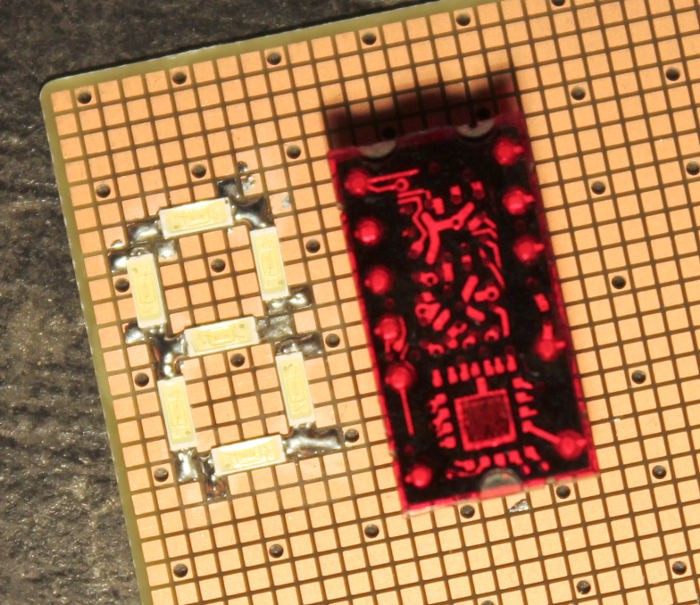
11/07/2015 at 09:13 • 2 commentsNever seen breadboards like this before (from @Yann Guidon / YGDES's https://hackaday.io/project/8121-discrete-yasep/log/27617-hexadecimal-7-segments-display-continued/discussion-40001):
![]()
The breadboard gave me an idea...
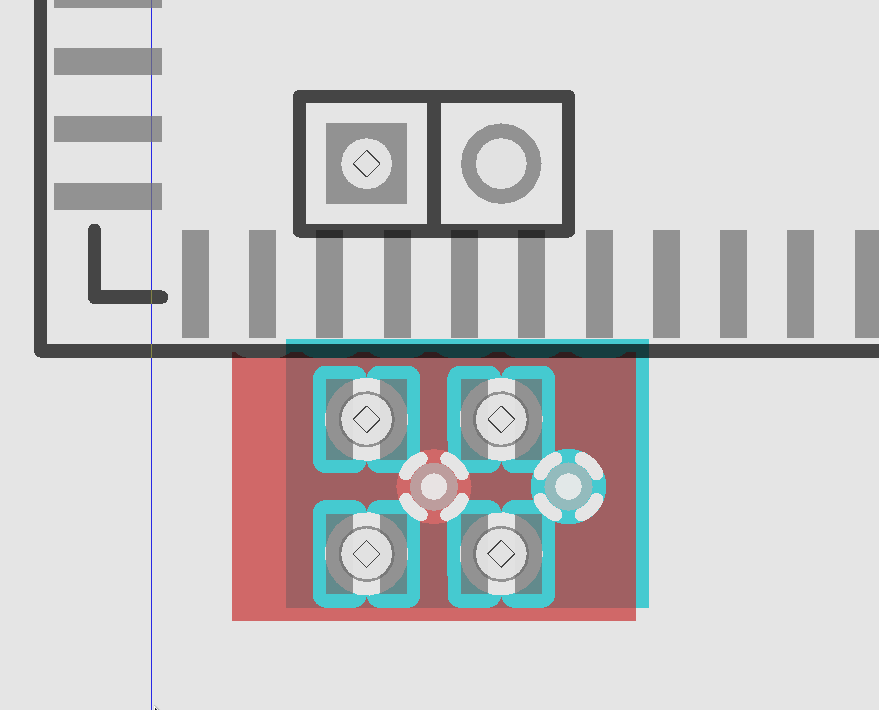
I usually like to work with through-hole parts on through-hole-plated double-side boards. But sometimes it's necessary to throw in a SMT part... One hack-job method I've seen (and have been using, when necessary) is to literally cut normal pads down the middle... That works surprisingly well on single-sided boards, but for double-sided through-hole-plated, you've got to also drill-out the through-hole-plating. Not a big deal, really (do the drilling-out first!) The hard part is cutting those pads down the middle, and do-so without ripping 'em off the board. And if you have to do a 16-pin device, that means 8 annoying cuts... What if the cut was already done?
This is some *really* early experimenting...
With normal through-hole pins, pretinning, and a little bit of flux, I imagine the pads would work pretty well as-normal...![]()
With surface-mount, the only necessary step is to first pre-drill the through-hole-plating. With the right drill-bit and a handle, this can easily be done by hand.
Some percolating thought-points:
Board-fabs seem to have differing/unspecified handling of THP vs non-THP holes. Especially with regards to holes that have no annular-ring (the bit of copper "pad" that surrounds a hole). So, the hand-drill bit would have to be big enough to rip that up, as well. (Or use another oversized bit as a countersink?).
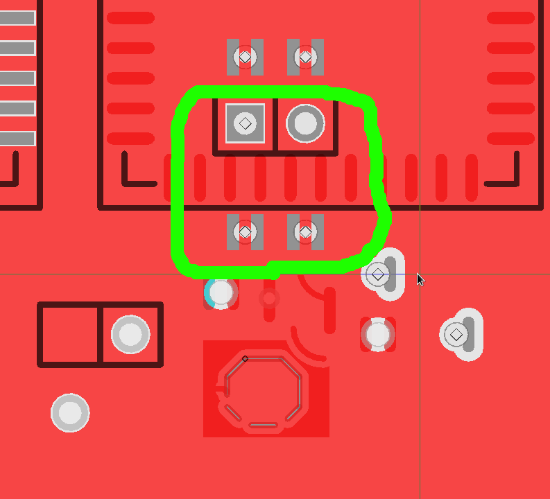
I also can't seem to figure out how to create surface-mount pads that are oddly-shaped... I'd prefer something more like half-circles, so vias can be placed diagonally between each .1in hole, while still allowing for current-flow on the two "planes" (usually ground and power):
And, obviously, I'm fighting a bit with clearances between the planes and pads as well as the solder-mask...![]()
But, it looks like it might work! I just grabbed the first part from the default libraries that had .05in spacing, it happens to be PLCC, which I seldom use... though it does make me wonder about whether something could be done for differently-directioned surface-mount pads...
And, then, there's also some consideration about higher-density SMTs... Maybe it'd be plausible to run four per normal DIP pad for 0.025in, but, the middle-pads would be cut-off by the hole... so, not sure yet. I'm obviously not opposed to point-to-point wiring on prototypes...
The same, then, would go for other spacings... but obviously those would have to be on a different area of the breadboard... Trying to keep this general-purpose, as well as versatile, yahknow.
Anyways, for only a couple hours' experimenting... it's looking promising!
-
Bare 486 chip...
11/06/2015 at 17:21 • 3 commentsUpdate: 11-6-15: Adding notes re: necessary pinout at the end...
--------------------
![]()
I've had this running thought to try to make use of various processors without actually writing code for 'em. And even, plausibly, not needing to learn too much about the processor/architecture to get it to do something useful.
The simplest example I've thought of, so far, is to turn a processor into a simple binary-counter... I'm not familiar with too many architectures, but I figure for many/most random old CPUs in my collection (Z80s, 8086s, 8051s, 6800s, mostly, but a few newer) it might be as simple as merely hard-wiring the data pins to a "NOP" instruction (and supplying a clock source). The idea, then, is the CPU will read a NOP, then advance to the next instruction, and do so repeatedly... Each time, incrementing the address output on the address-pins... Then the address pins are a binary-counter. Done. (Right?)
(TODO: link the dude who figured out how to create moody-faces via floating "instructions")
So, after years (more than a decade!?) of percolation, I finally started this crazy venture, and for some crazy reason I decided to start with an Intel 486 chip. (I dunno squat about low-level x86 stuff, certainly not assembly-level).
Some initial nicities; noticed, as well as later discovered:
The PGA package is 0.1inch-spacing. Cool.
I have several floating 'round.
The data/address bus is apparently pretty standard... It uses parallel TTL-level signals, and doesn't do any sort of strange multiplexing that would require additional chips such as a latch...
(I'm not certain about other processors, but I have an inkling some of the newer ones might have sophisticated busses that would be quite a bit more difficult to hack without e.g. a "bridge" chip... apparently I lucked-out that the 486 doesn't seem to require one).
Managed to find the 396 page scanned-datasheet online (the PDF claims DataSheet4U.com, but I'm pretty sure i got it from a different domain).
Thankfully there's a pretty decent overview of the pin functions, and despite there being 168 pins, there aren't *really* that many different ones to learn about. The vast-majority are Power, Data, or Address. But there're some control signals that need to be tied to certain levels. E.G. to avoid triggering interrupts. There are a few features which I don't care to make use of, cache configuration, etc. that need to be understood at least well-enough to disable their functionality. Thankfully, the "Quick Pin Reference" table is clear enough to figure out what levels to set these to, so I don't have to dig into the intricate details of a function I don't care to use.
Another input indicates the byte-width of whatever "device" it's talking to. Does the BIOS-ROM have an 8-bit, 16-bit, or 32-bit data-bus? What about the RAM, or the ISA card...? That's handy, the NOP instruction (also found in the datasheet) is only one byte, so maybe I can get away with only "hard-wiring" 8 signals rather than 32... (though, of course, floating-inputs is generally a "bad" thing, this is DEFINITELY a hack-job).
There's also one pin to signal that the "device" is currently feeding the data on the lines and the data is ready to be read by the CPU. This one... I might have to come back to.
Oh, Reset and Clock, of course...
Again, luckily, the 486 still uses "easy" signals ... the clock input is a single TTL-level pin. Specs claim it's only guaranteed down to 4 (or 8?) MHz, but elsewhere they claim it was designed to run slower, just not tested... so that'll be a test for the future. Note that the 486DX processor I'm using doubles (or triples?) the clock-speed for internal-use... That means the clock signal has to be "stable", it probably won't work with a pushbutton to "step" the clock. Earlier 486s didn't have this, so they might even be pushbutton-steppable. (TODO: Note Re: clock-multiplying and the effect on actual execution when instructions can't possibly be read at that speed?)
Reset is supposed to be active until the power and clock have stabilized... I thought, maybe, I could get away with a technique I'd seen on an 8051 circuit... Simply, tie a capacitor between V+ and the reset line, then a resistor between reset and ground... Choose a large enough time-constant that power and clock start-up times are negligible. (I used a 33k resistor and a 10uF capacitor).
![]()
Now, here's where I'm at:
First: The processor doesn't seem to *start* all the time, but sometimes it does.
I *think* this might have to do with the reset-input. I haven't yet looked into the timing diagrams, but a slowly-rising reset input, combined with electrical noise (e.g. 60Hz) might have something to do with it. From what I *have* looked at, so far, I recall seeing something about reset having to be active for 15 clock-cycles, lest things be in an "unknown" state...
Well, here's what I'm visualizing, anyhow... This is a *processor* not a *microcontroller*, so it's designed to be in a somewhat more "ideal" environment... I haven't checked, yet, but the reset input may not have a Schmitt-Trigger, in which case, the slowly-rising signal may be near the trigger-value long enough for additional electrical-interference to cause it to "bounce" around the trigger-value a few times... So, that's one possibility. There's also the possibility that the reset input fans-out immediately to different parts of the processor, one may have a slightly lower threshold-voltage than the next... Neither of these "theories" would be problematic if the reset signal switched within a single clock-cycle... and it may well be that most motherboards have a synchronously-clocked flip-flop to do-so.
So, that's one thing I'll be looking into.
Second: When it *does* start, the lowest address-bit (bit 2, oddly) isn't toggling at a rate I would've expected.
I'd already kinda figured there may be some funkiness with the processor trying to execute instructions at twice (or thrice?) the speed they can be read... So, I did kinda expect that the lowest address line might not toggle with every clock-cycle. But, wouldn't it be consistent, and the higher address-bits would appear to toggle at 50% duty-cycle...? Well, they don't, and that's weird. Oh, and A27 never toggles, which is also weird... (to me).
So, first, I found a bit about the boot-mode of the CPU... I don't fully understand the details, but something about: It starts at 0xffff fff0, where it expects to see a jump instruction to somewhere within the first 1MB, which is where the BIOS-ROM is generally located. OK, but if it doesn't find a jump, and instead finds a NOP, wouldn't it just continue to the next addresses and eventually wrap-around to 0x0000 0000?
I dunno, because the next bit I found says that after the expected "jump" the system limits itself to addresses within that first 1MB... So, then, that might explain why I don't see any toggling on A26.
Great. So, if I don't learn how to program this thing, my binary-counter might only be, what... 12-bits? Oh well, still it'll do *something* plausibly-useful, and that's what I'm after...
So, I'm still confused about why the toggling of the bits doesn't seem to be occuring at a regular rate... And it occurs to me: What if, for some really weird reason, the processor attempts to write data *to* the data-bus (maybe not actually intending to write to a *device*)... I don't know *why* it would, but then again I don't really understand quite a bit about this architecture... (How the heck does "caching" make any sense?! Who tells it what to cache? And what's it do when it's twiddling its thumbs because it's waiting for data on its slow bus? etc. etc. etc. Could it be attempting to send an "error code" to some outside "device" that isn't implemented...? I dunno...)
I'd set up my "hard-wired" NOP via pull-up and pull-down resistors... Mostly thinking that I might choose to wire up something else later (like, maybe, a ROM, plausibly filled with instructions? Crazy, I know). But, it looks like it was a good thing I did it that way, rather'n wiring the data pins directly to VCC and GND... Because, indeed, after scoping it out, sure-enough there's data being driven on that Data Bus, despite my "hard-wired" NOPs.
Whew. Where's this leaving us...?
It's there, and the NOPs are getting mangled because of the internal-capacitance in the CPU's Data pins, combined with the resistors... It clearly takes on the order of 100 bus cycles for the resistors to "recover" from being driven. OK...
So, logically, the CPU, at some point, appears to be sending data to the bus, for some weird reason (plausibly due to oddities in the reset-process, as well as a multitude of other plausibilities, many of which may actually be *proper* functionality that I just don't understand). WHEN that happens, the next instruction that's read is *definitely* mangled. Who knows what it's doing at that point... It could be jumping to another address, or doing math on random values, or who knows.
But... often, it seems to be *repetitive*, whatever it's doing...
And, interestingly, the pattern seems to be different each time the CPU's reset.
Here's where I should just stop... it's kinda cool, really, a randomly-generated pattern that repeats... Maybe if it runs at low frequencies I could assign a percussive instrument to each bit... hmm...
But, of course, I've troubleshooting in my brain, so I've obviously been thinking about ways to solve this "problem"...
(Which is kinda ridiculous, 'cause what am I going to do with a 12bit counter that's stuck at a fixed frequency that I wouldn't just do with a chip designed for that purpose? The whole point was to make something "useful", but "useful" could just be "interesting"... that "Moody-Face" thing is pretty durn cool, and it does it with the utter-randomness of *floating* inputs)
But, of course, I've troubleshooting in my brain, so I've obviously been thinking about ways to solve this "problem"...
And, I have a few ideas...
A) Clean up that reset. Plausibly, if it resets in the "right" state, it will read the NOPs as expected and never drive the bus and get "mangled" instructions in the first-place. (Plausibly). Schmitt-Trigger (+ D-flip-flop?). Done.
B) Maybe driving the data-bus is something the CPU is *supposed* to be doing... I dunno it that well. So, what can be done about that...? Well, there's the "Ready" pin, and an output pin from the processor saying when it drives the bus... or another output pin from the processor saying when it wants to read from the bus... So, another R/C delay (possibly another Schmitt-Trigger/Flip-Flop) with a time-constant that's longer than the time it takes for the resistors to "recover". Done.
This also presents another interesting path... Maybe the CPU won't run at pushbutton *clock*-speeds... But, what about this "Ready" pin... could *that* be slowed down dramatically...? The next instruction is requested one clock-cycle after the last one was executed, but then it doesn't actually *receive* the next instruction until... maybe I set the R/C time-constant to a full second later, or maybe not until I decide to push a button. hmmm....
What *am* I making with this thing, anyways?
--------------
Update 11-6-15:
Here's the PGA-168 pinout... This is *nearly* identical for all 486 PGAs... (486, 486SX, 486DX, DX2, DX4...)
But they do differ, slightly. They should, however, be compatible, as the differing pins are usually added to old N/Cs and usually have internal pull-resistors for default backwards-compatibility. But, definitely look at the datasheet, section 3. This contains pinouts, descriptions of the pins, and also contains a table which shows the differences between different versions of the chip. My circuit's a 486DX-50, but my initial research was for a 486DX4-100, so there's a bit of notes re: both parts. Sorry it's so blurry, if you're really interested I can scan it for yah, lemme know.
![]()
Random Ridiculosities and Experiments
Sometimes yah's just gots tah try somethin', regardless of whether it'll become a full-fledged "project"...
 Eric Hertz
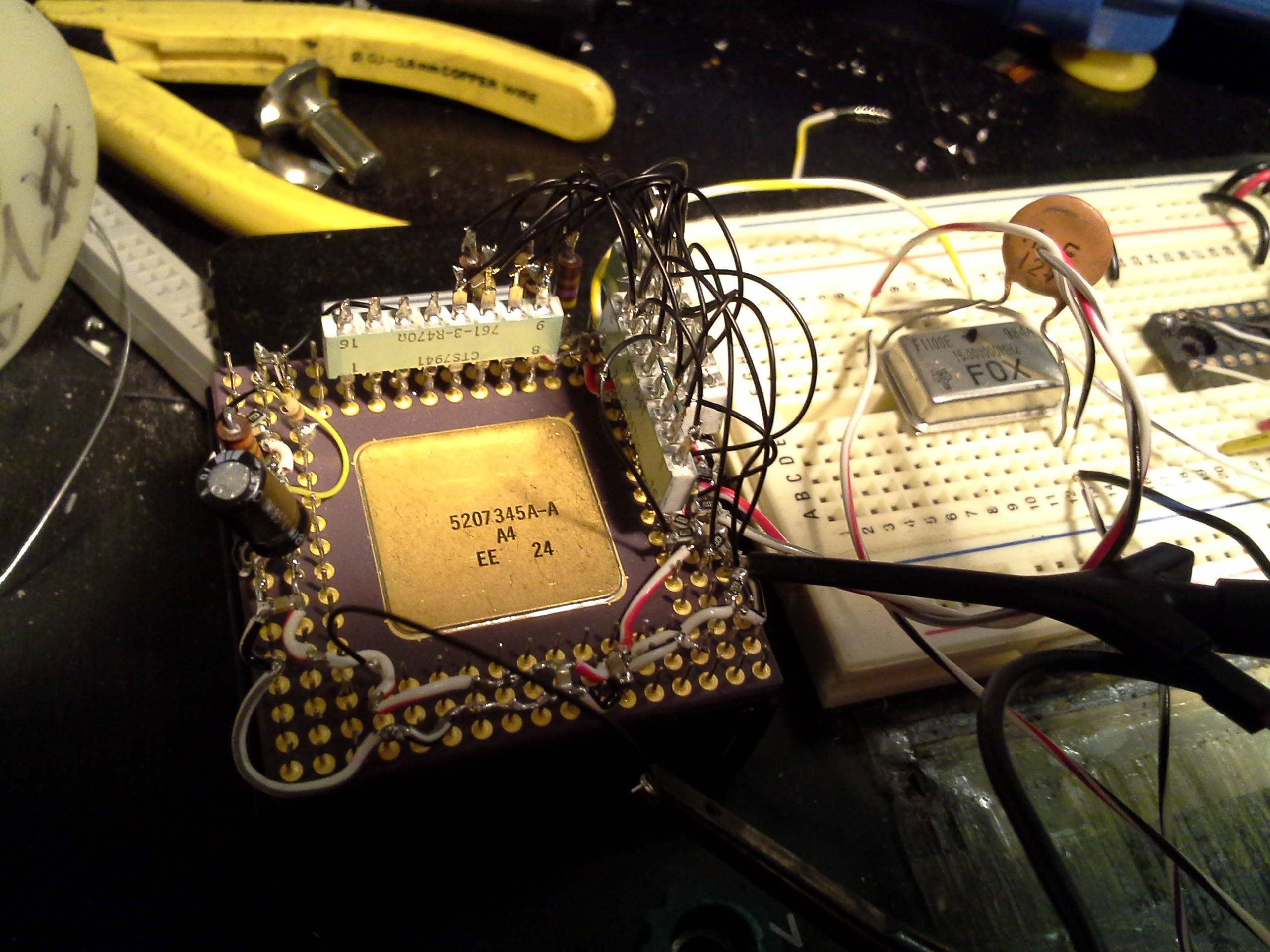 I used straight-through DIPs, and bent the pins straight out the packages...