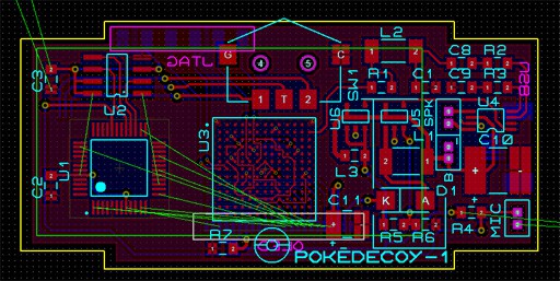
Yesterday, I noticed (too late again) that OSH Park couldn't handle the trace width required for the CPLD routing. As I didn't want to have both special trace width and inner-layer requirements, I'm trying to keep the board only 2-layers to go for PCBCart's prototype service.
They do 4mil/4mil traces and 13mil vias for a reasonable price.

SPI flash, JTAG, switch, power supplies, and audio section are done.
 Furrtek
Discussions
Become a Hackaday.io Member
Create an account to leave a comment. Already have an account? Log In.