I would like the gates to consume little power, ideally around the 1mWballpark. Most gates run in the 10mW range (and more, @Tim got to 44mW and that's still an order of magnitude too high for my tast, sue me).
I would like to use the AF240 : PNP Germanium metal-canned transistors, because that's badass.
To fulfill the 1) and benefit from 2), I set the power supply to 1.5V. Though it could be lowered later but Falstad doesn't let me use a Germanium model.
I drop the Baker clamps. Instead I try the "non-saturating" approach of ECL and LVI and this is where things become interesting. In fact it looks quite a lot like a HF inverting amplifier stage and in the end, that's pretty close to what we do, right ?
I drop the choice of ECL because the power supply would be too high (due to several factors). Instead LVI is a bit simpler and a bit less fussy.
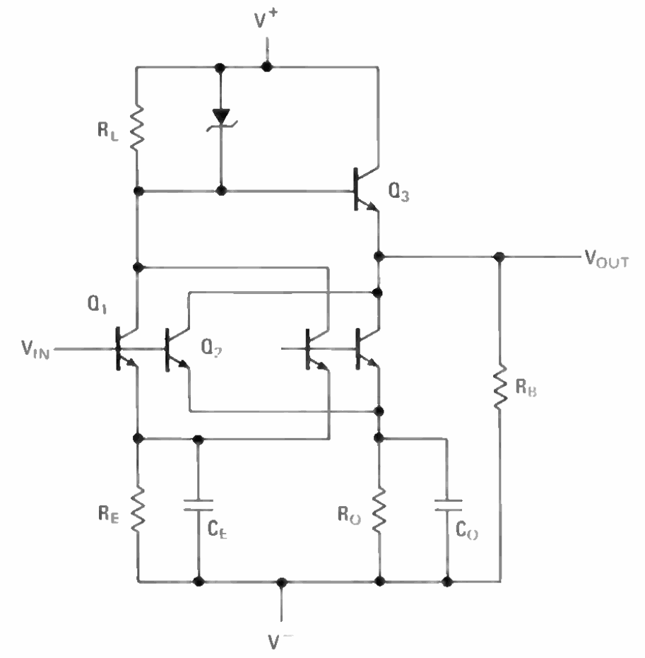
LVI gates have been already studied and it's interesting because it's easier to tune for a given power draw point. The first thing to observe is that a LVI gate combines 2 sub-parts :
A classic inverter
A 2-transistor amplifier with emitter-follower output.
The cool aspect is that both parts reuse more-or-less the same design for the parallel transistors (with shared base). So I can start to design the inverter first, set a given power draw, and duplicate it for the emitter follower half.
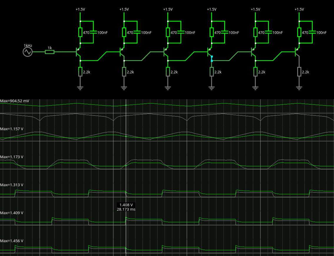
So this almost acts like an inverting amplifier with a swing (in this very case of fanout=1) of 550mv-1100mV (centered around 850mV).
The base current is limited (to about 500µA) by the 2.2K resistor of the previous stage. The other resistor is set to 470, and together they limit the overall current. There is no direct path to ground so the power can be kept in check.
The 470 resistor is pretty critical, not just to set the working point. It also provides some degeneration, which increases the sensitivity of the base, giving the above 550mV logic swing. Furthermore the capacitor adds some more hysteresis, increases the gain temporarily, its value should not be too small (above the equivalent Miller charge, and I don't count fanouts). The overshoot on the traces above are good signs. This "boosted degeneration" is characteristic to the LVI gates and I have not seen it in other discrete deconstructions/reconstructions. Maybe this could help the DCTL gates too ?
My concern is that the Germanium transistors have a lower Vbe and possibly a smaller swing, and I can't simulate it with Falstad's Circuitjs. I'll have to try by myself on the bench, maybe by increasing the 470 to 1K. The maximum draw I want on the 1.5V supply is 2mA, and for now I measure 750µA in active state, or 1.3mW, which amonts to 0.65mW in average.
_______________________________________
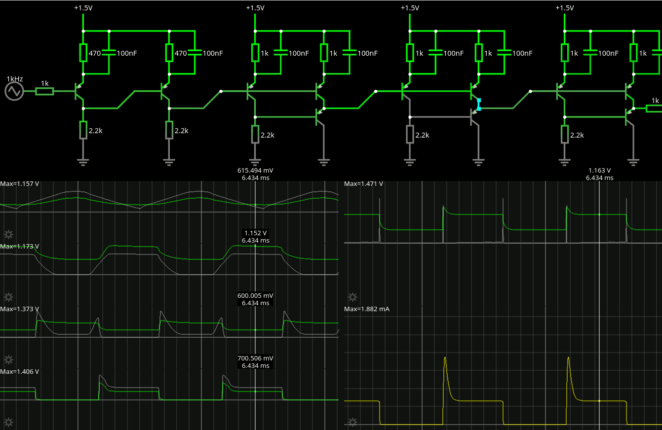
The next step is to duplicate the inverters, so the 470 is doubled to 1K to keep the base current low. The low Vcc is great because the resistors still have a rather low value, reducing the output impedance while also reducing the power losses through the resistors.
The above gate has a max. draw of 1mA, or 1.5mW (0.75 at 50% duty cycle), it's quite good so far, but the 2.2K resistors must be deduplicated. Adding the emitter follower brings the new topology:
the yellow trace at the bottom is the supply current : it peaks at 1.8mA but settles to 650µA, that's right 1mW !
The emitter follower has a swing that exceeds 0.7V, indicating saturation, so a diode could smooth this a bit and prevent transconduction of the push-pull stage. Adding a 1N4148 increases the plateau to 750µA and the peak to >4mA so the speed benefit better be significant. But I don't see a significant difference. Another more interesting effect is obtained by setting all the resistors to 1K, as this helps discharge the base faster from the emitter follower.
I can play with Vcc, measure the inverter's power, compare the reactions with various capacitances... The push-pull's capacitor helps increase the swing but the other one can be a bit larger, though being equal is good too. The push-pull works nicely when dealing with capacitive loads (such as long wires). The boost capacitors must be at least equal to the load.
The signal swing is about 400 or 500mV, which is not much but cascading the gates seems to be OK (I observe the 3rd in the chain to make sure the signal characteristics are pertinent, input and output).
The above circuit seems suitable for use with high speed bipolar transistors (like BFS480 or BFP420) but the speed must be measured, without and with capacitors of various values.
The AF240 would run at 1.3V or 1.25Vcc so I can regulate with a LM317 directly. I'll have to compare the latest version with the original "balanced" inverters, to see which is fastest. Saving a couple of transistors would be nice right ? but LVI shines when the output load increases so higher fanouts become possible.
I had no clue at first because no resistor value was hinted in the schematic. After some falstading, I think I got the idea and let's redesign it from the ground up, using the fundamentals.
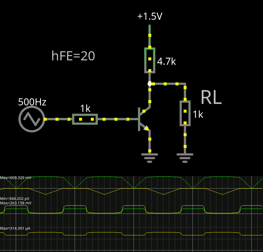
Let's go back to the old good RTL (Resistor-Transistor Logic) family with the basic inverter :
It's sweet and simple but has many drawbacks. The DCTL family was designed to overcome some of them but the pull-up part is the nagging part that forces power/speed/fanout constraints. In the example above, the output level is crumbling under the load of RL that is lower than the pull-up resistor. So the pull resistor is often quite low, which increases dissipation a lot. And if the resistance is higher, the downstream circuits will switch slowly.
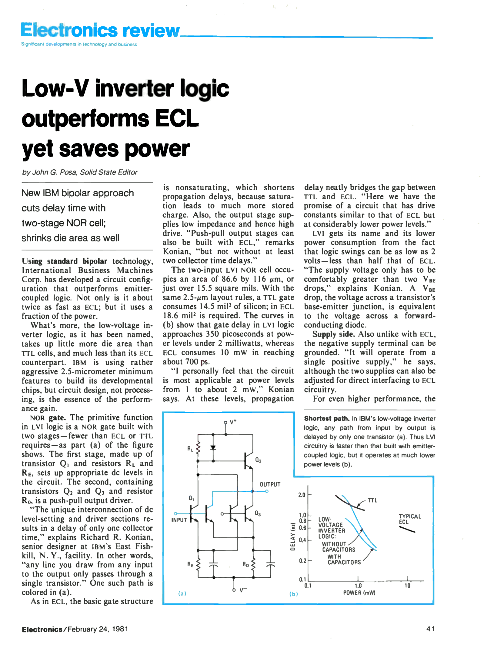
Even with ECL, the pull resistor at the output is pretty concerning and IBM notes that ECL signals must go through 2 emitters, which also limits the speed, but ECL introduced "non-saturating logic" that increases the speed. So IBM tried to combine a pair of favourable features.
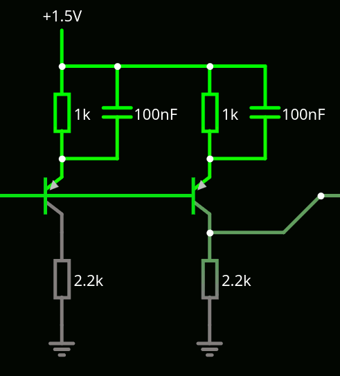
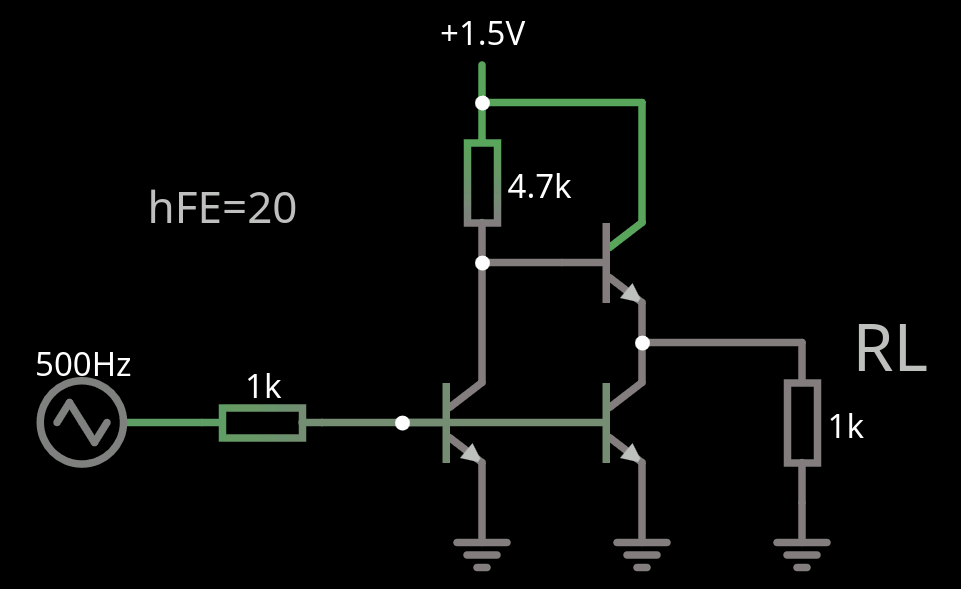
The first thing is to remove the pull-up resistor and swith to push-pull topology. For this, 2 more transistors are required : the first is a high-side common collector (like ECL), and the second is directly tied to the input, to control the base of the emitter follower.
There are 2 transistors doing the same thing in parallel (sharing the same base) because they drive different things that would not work if tied together. So we get to the 3-transistor push-pull:
It's more efficient but now there are 3 semiconductors so it was not considered in the first era of computing because of the price of a single transistor. In the late 70s, the cost per junction had started crumbling to a level that made this possible (as the ECL boom has shown).
There is no significant difference on the traces because the RL is too high, and the speed too slow to show any parasitic effect... Also due to the emitter follower, the output can only go up to Vcc-Vbe, or about 0.75V in the above example. It's higher than the 0.26V of the first example but under a low Vcc, the swing is narrow...
But 0.6V of data swing is good enough if the circuit works at low voltage because this also reduces the power draw (as seen in the DCTL experiments of the previous years). Power is turned into heat and a lot of problems so working with low voltages is good (and this is even better with Germanium transistors hahaha).
The next step that IBM took was to turn this gate into a non-saturating circuit. There, it gets to another level of analog wizardry but experience with ECL helped me unravel this a bit.
The point of avoiding saturation is to keep the transistor able to switch as fast as the input signal, and saturation stores charges in the Miller equivalent capacitor of the base. The 2N2369 was designed to reduce charge storage but this did not scale in higher frequencies and other parameters. So the transistors must be kept in a sort of equilibrium, which consumes current, but not too little or too much. The absence of resistor values in the only schematic available was annoying... I also chose low-hFE transistors because it tends to decrease with the speed (and/or the current). The germanium PNP AF240 has a hFE around 20 or 30 so it should be representative.
A particular detail of the original schematic is the diode in parallel with the resistor : this limits the output swing as well as the saturation (I suppose). That's the key to any change to the input-output level compatibility because the clamping must be changed when the Vcc is changed. For now I have chosen 1.5V but at 2Vcc, a second diode is required in series.
I was not able to meaningfully test the interaction of the RC cells at the legs, I suppose that the diode makes the emitter resistors conduct more current and shift the base (degeneration), keeping the input from saturating the transistors. Also I don't know why the RC are duplicated, maybe to fine-tune the values and reduce the power.
So the next schematic is the previous one with 1 more diode and 2 emitter resistors. The capacitors become meaningful at very high speed so I don't show them at such a low speed.
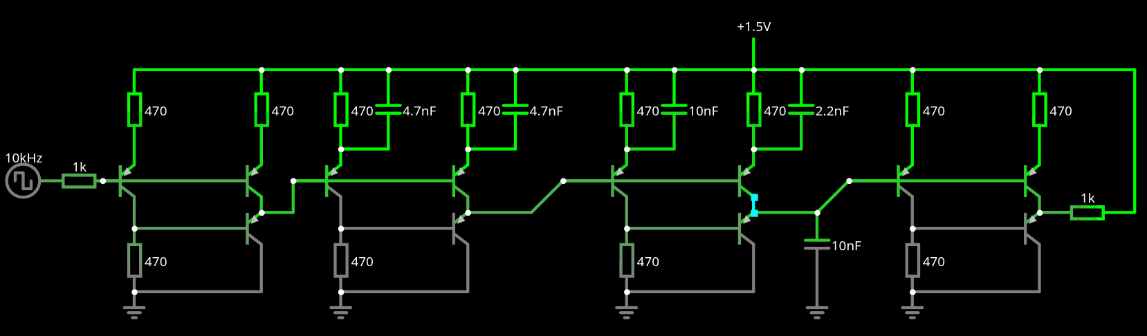
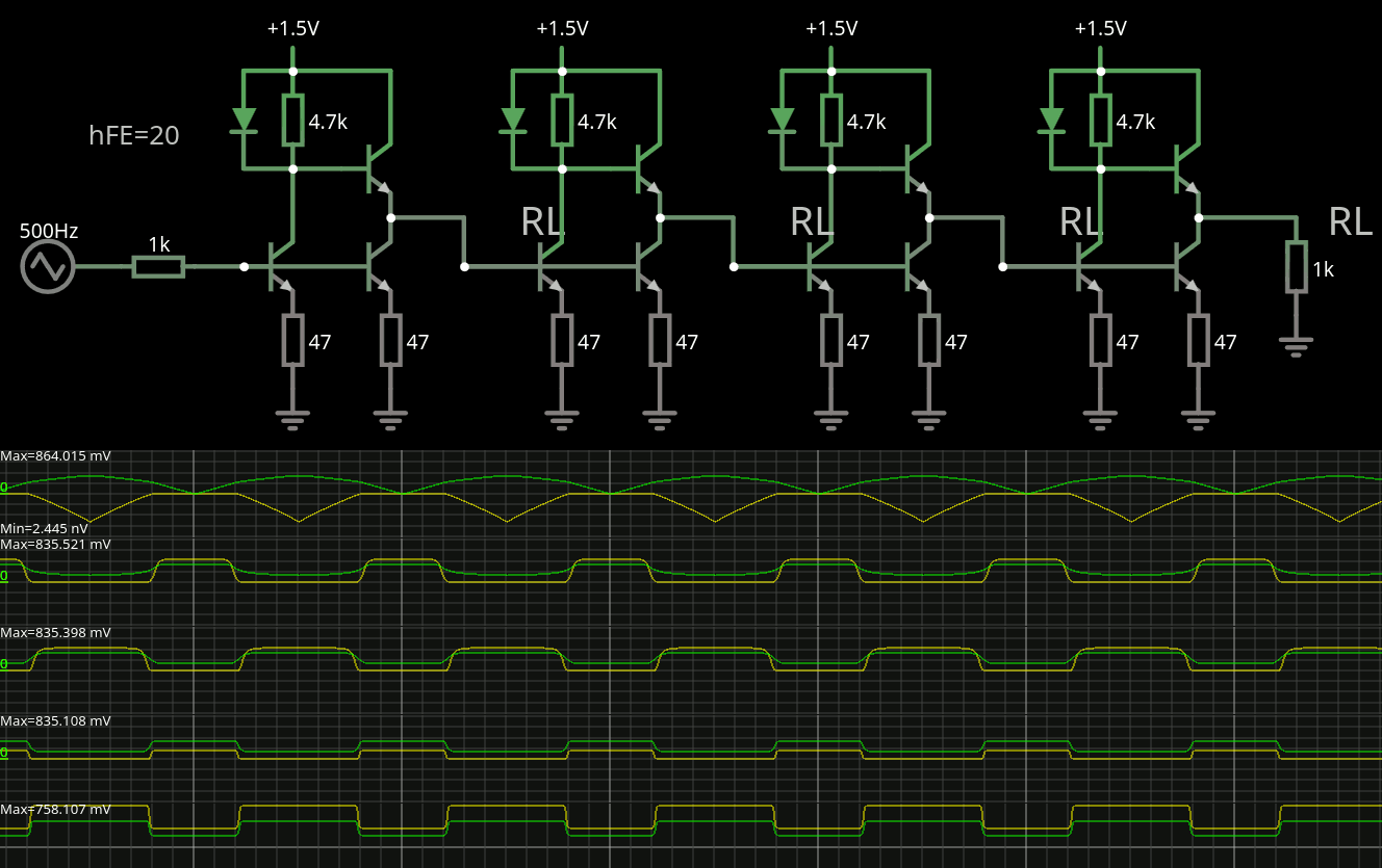
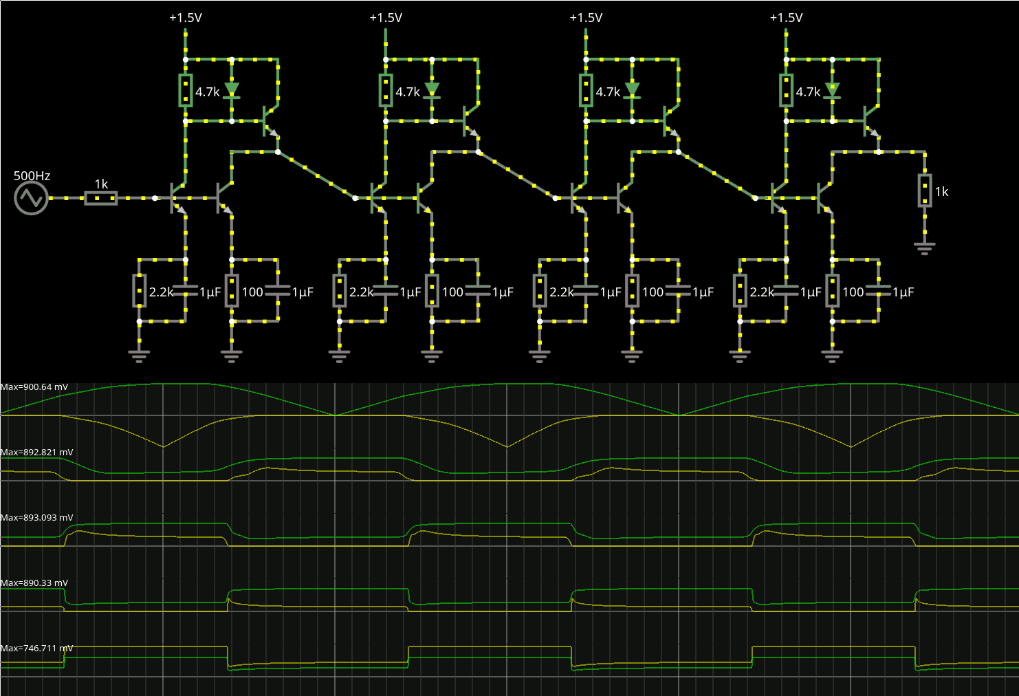
The following circuit chains 4 LVI inverters to ensure that impedances are matched:
The signals swing from 346mV to 835mV. The input is a triangle (current-limited by a resistor) that gets correctly reshaped by the first inverter stage. The last stage is a pull-down load that shifts the swing down to 344mV-758mV with 758µA.
The output levels seem reasonable and quite stable. Input current is about 430µA for high level, and almost 0 for low level.
The problem is the diode that passes quite a lot of useless current and each inverter is pretty greedy, at least with the above values of 47 ohms per degeneration leg.
There are 2 ways to reduce the current : drop the diode, and the Vcc can go even lower. There is a risk of saturation though. But the power is greatly reduced.
Or increase the Vcc and increase the degeneration resistors to limit the diode's current and... This reduces available current for output. That's where the capacitors enter the stage to compensate during the transients. The gates are rated by IBM at around 1mW under 2V approx. That's 500µA max per gate.
The pull-down transistor should have a low resistance to ground to quickly drive the output low. Let's try 47 ohms. However the diode side should limit the current to 0.5mA and the diode drops 0.6V already so R=U/I=1.4/0.0005 or 2.8Ko ohms. And that's where I see that the leg resistor of the leftmost inverter can be greatly increased.
The presence of the diode increases the current but also greatly reduces the signal's swing and that's probably one key to keep the transistors in the linear region : faster speed comes from less swing and little stored charge. But now the signal integrity is harder and the imbalance of the resistors creates a new concern : the upper and lower sides should now be able to conduct at the same time. Watching the current from Vcc shows the system is safe though.
The type of diode also has an effet : low-voltage High Frequency type (low capacitance) is required, since the gate is advertised in the 200ps range... Even selecting the 1N4148 in the simulation affects the waveform compared to the "default model".
Falstad's circuitjs is not suitable for high frequency simulations so I can only check the power, logic levels, waveforms... I can cheat by adding large capacitors for example but SPICE and real circuits will give the definitive answers.
Here are the waveforms with 4 inverters with diodes: Each inverter draws either 3mA or 230µA @1.5. That's maximum 4.5mW per gate, still 5× the promised consumption but that's 10x better than the 44mW reached by log 24. Beyond 2ns with 2N2369A.
Of course the values are not "right", I focus on the resistors to get the proper working point. The capacitors will have a small value, probably in the tens of picofarads, equivalent to the Miller capacitance of the transistors.
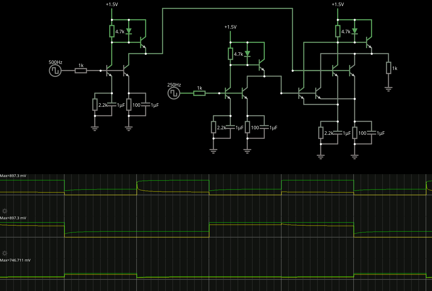
The waveforms above show that the edges are rectified and enhanced, from the altered triangle to the clean edges of the last inverter.
To ensure a proper input level, I reused the inverters for impedance adaptation. Here is a more succinct version : the degeneration resistors are 1K5 and 330, the lowest resistor sets the maximal static current (here about 1.3mA, or 2mW). The capacitor will affect the dynamic behaviour.
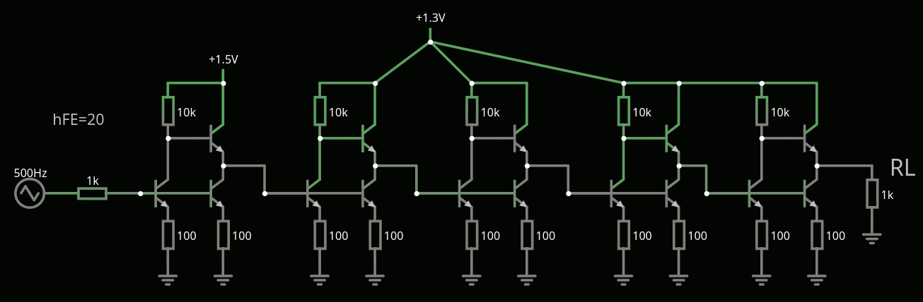
Of course NOR3 has 3 pairs of transistors. I hope that the initial schematic is now easier to understand.
That's mind-boggling. I have never heard of this or seen it before. It works with identical polarities of transistors, which simplifies the design compared to some types requiring complementary parts (NPN+PNP), lowering the cost.
I'm sure the other TTLers will want to have a try with the types of transistors they have : either 2N2369, or AF240, or just dumb BC548... Of course one must verify that this works with discrete transistors.
NOR2 requires 5 transistors, it's a 2N+1 count so it increases faster than ECL but even a NOR3 is worth the effort. Unlike ECL there is no complementary output though, so certain logic simplifications are not possible... So it's only NOR, like in the old-good-CDC6600. Which raises the question of how to make a suitable DFF.
In his log Pushing RTL to <2 ns Propagation Delay, Tim alluded that a combination of base capacitor and base-collector diode could reach 2ns of transition time per inverter.
Well, @Tim, it wasn't that hard after all ;-) How about 1.73ns at only 5V ?
OK it's ugly (bad baaaad probing) and the CDC levels are pretty much destroyed...
But it's FAST and even more POWER EFFICIENT !
I get 32MHz at 5.2V and only 77mA, or 44mW per gate, a 4.5× improvement compared to Tim's 200 mW :-)
What's my secret ? Not much, it's explained in the previous logs ;-)
ample capacitor decoupling
low Rb (150 Ohms)
finely chosen Cb (68 pF)
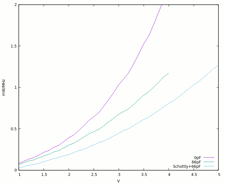
But this log has a newcomer : a Schottky diode. Spoiler alert : I didn't pay much attention, I found 2 reels of SMB and SMA-packaged low voltage diodes in my drawers. I don't even remember where/how/when/why I obtained them but here they are !
This version uses a ROHM RB751V-40 Schottky barrier diode in a tiny tiny package (almost 0603). It's limited to 20mA which matches well because the higher the current, the larger the junction, the more capacitance...
I also have MBR0520 diodes but the higher current rating potentially increases the capacitance, which would create more problems.
The 2N2369A is prevented from "switching hard", which has a welcome effect : less current is drawn ! At 1V the circuit sips only 3mA instead of 6mA... By 2V the difference is mostly erased, though, but at low voltages, that circuit is crazy efficient :-)
set xlabel 'V'set ylabel 'MHz'set y2label 'mA'set xr [1:5]
set yr [6:36]
set y2r [0:90]
setkeyright bottom
set y2tics 3
plot \
"ringo9v2_0-68pf-RB751.dat"using1:2 axes x1y2 title "0pF current in mA" w points pt 7, \
"ringo9v2_0-68pf-RB751.dat"using1:3 title "0pF frequency in MHz" w lines, \
"ringo9v2_0-68pf-RB751.dat"using1:4 title "66pF frequency in MHz" w lines, \
"ringo9v2_0-68pf-RB751.dat"using1:5 axes x1y2 title "Schottly+66pF current in mA" w lines, \
"ringo9v2_0-68pf-RB751.dat"using1:6 title "Schottly+66pF frequency in MHz" w lines
From there we can also plot the power/frequency curves with the following script :
set key right bottom
set xlabel 'V'set xr [1:5]
set yr [0:2]
set ylabel 'mW/MHz'
plot "ringo9v2_0-68pf-RB751.dat" using 1:(($2*$1/$3))/9 title "0pF" w lines, \
"ringo9v2_0-68pf-RB751.dat" using 1:(($2*$1/$4))/9 title "66pF" w lines, \
"ringo9v2_0-68pf-RB751.dat" using 1:(($5*$1/$6))/9 title "Schottly+66pF" w lines
The result is self-explanatory :-)
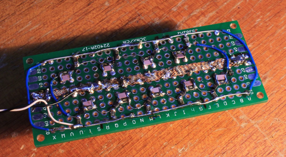
These curves were measured on this simple board :
What else is there to say ?
It's not the end of the adventure, of course, because it's only a ring oscillator and the diodes have destroyed the saturating "CDC levels". A clean PCB would help too, but mostly the problems come from multiple inputs driven by one output.
Oh, one last word : the 2N2369 is very cool and easy to use when you understand a few tricks. But there is one design flaw : the can is connected to the collector, not the emitter :-( At least the SMD versions use plastic cases that don't create short circuit hazards.
set xlabel 'V'
set ylabel 'MHz'
set y2label 'mA'
set xr [1:5]
set yr [6:24]
set y2r [0:90]
set ytics 1
set y2tics 10
set key right bottom
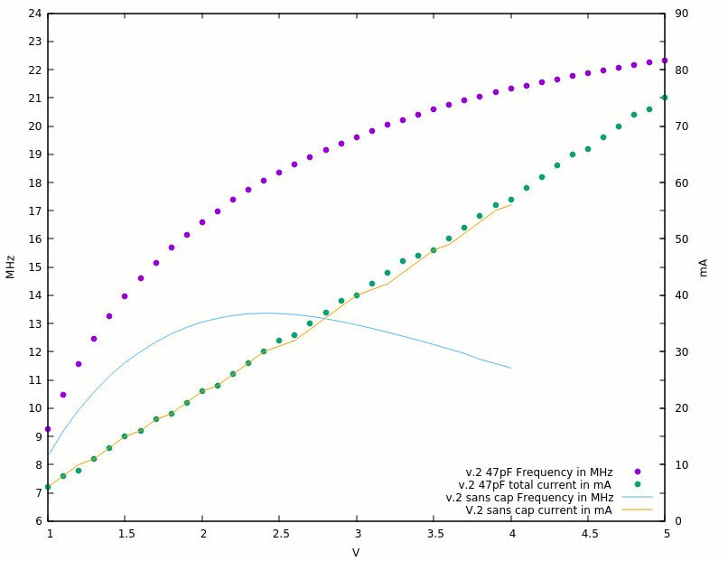
plot "ringo9_2_47pF.dat" using 1:3 title "v.2 47pF Frequency in MHz" w points pt 7, \
"ringo9_2_47pF.dat" using 1:2 axes x1y2 title "v.2 47pF total current in mA" w points pt 7, \
"ringo9_2_sans.txt" using 1:3 title "v.2 sans cap Frequency in MHz" w lines, \
"ringo9_2_sans.txt" using 1:2 axes x1y2 title "V.2 sans cap current in mA" w lines
Once again the capacitor is a simple yet very effective means to go faster, yet the power curve is not affected (in a meaningful, significant way). So the efficiency is much better than v1 :-)
At 5V the circuit easily reaches 22MHz, or 2.5ns per inverter !
But is it necessary to go THAT fast ? Where is the sweet spot again ? I don't think it's a good idea to run at 5V because the speed is only marginally better for a very significant increase in power draw (42mW/gate, or 1.8mW/MHz). So maybe 5V would be reserved for special cases and places that need a serious fanout.
2V : 46mW => 5.1mW/gate, or 0.3mW/MHz/gate
2.5V : 80mW => 8.8mW/gate, or 0.48mW/MHz/gate
3V : 120mW => 13.3mW/gate, or 0.68mW/MHz/gate
3.3V : 152mW => 16.8mW/gate, or 0.83mW/MHz/gate
5V : 375mW total, 42mW/gate, or 1.8mW/MHz
It would be wise to stay under the 1mW/MHz/gate, 0.5mW/MHz/gate would be even better but the fanout would be insufficient. The standard voltage 3.3V would be a good compromise but let's wait for the results with the other cap values and the diodes !
Anyway : Going from 2.5V to 3.3V brings only 10% more speed while the power almost doubles !
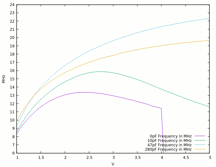
But what is the right capacitor value ?
the datasheet specifies < 4pF for the gate charge. So the capacitor must be higher than that to cancel the effect. So maybe 47pF ?
OTOH I saw a speed difference that is similar between 27pF (PCB v.1) and 47pF (PCB v.2) so there would be a diminishing return, which can only be spotted by plotting the V/F curve with various capacitances.
The smallest capacitors I have are 10pF so that's a good start. I can then add 18pF in parallel to give 28pF. Adding 47pF again will give another trace...
The results for 10pF are below :
From this graph, we can only suppose that the next increase would be to 220pF...
Meanwhile, the current graph has not changed so I don't show it anymore.
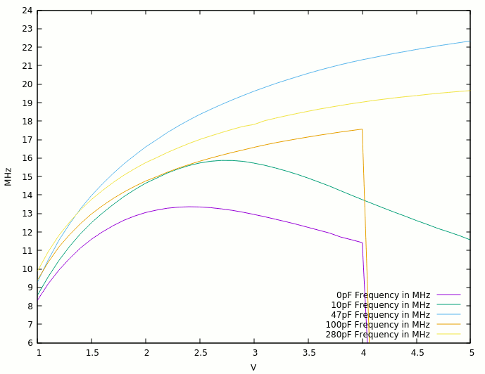
Testing with 280pF gives a pretty unexpected curve, but good to know anyway :
After a promising start at very low frequency, the 47pF curve is already winning at 1.4V. I now have to check at 100, 68 and 33pF if there is another local maximum...
The 100pF curve is disappointing : why is it worse than the 280pF ?
What is so special about the 47pF I tried ? Did I fry a part ?
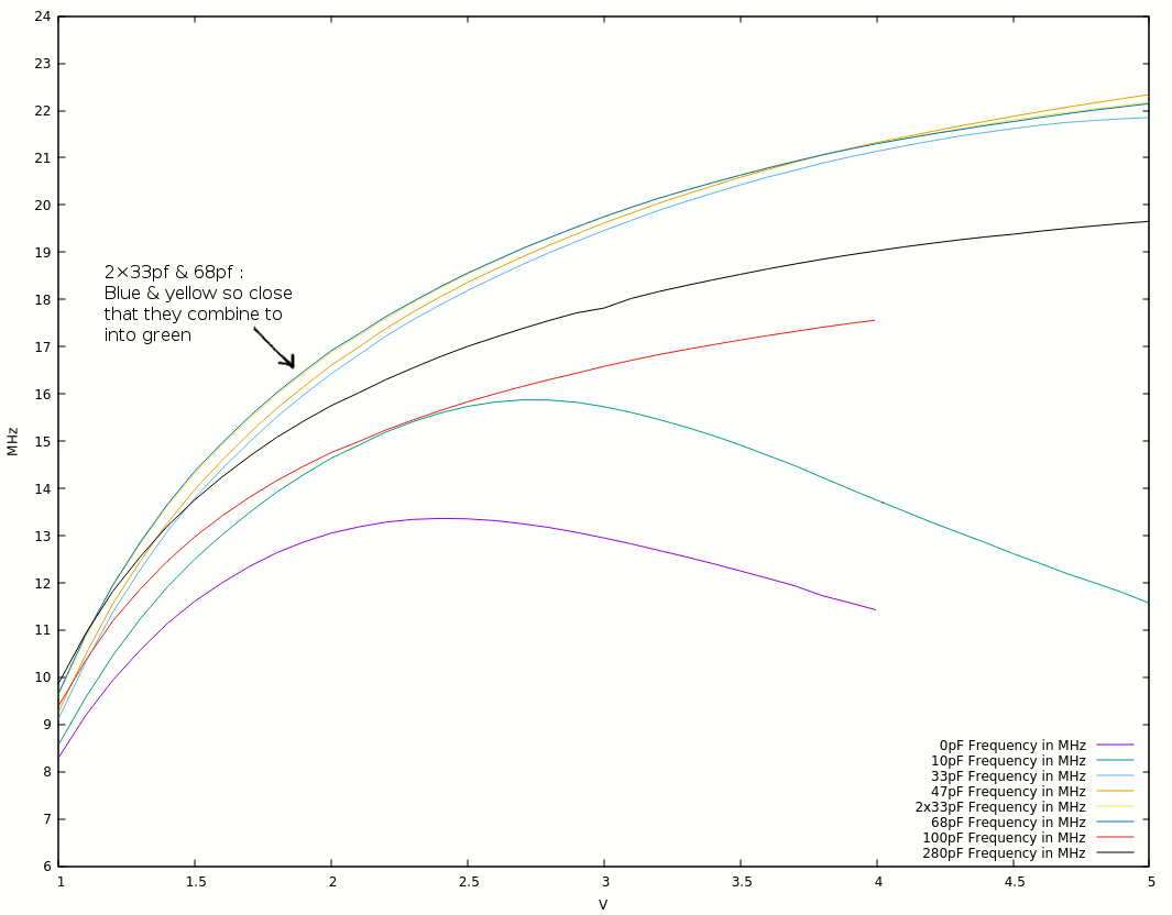
Trying with 33pF caps shows interesting results as well, close to the 47pF.
Apparently the 2×33pF combination has a very light advantage up to 3.5V : that's still good to take and much better than other values.
Now trying 68pF gives a result very close to 2×33pf. So close that gnuplot almost mixes the colors, unless you zoom a lot.
So 68pF wins by a tiny margin, but that's all I intended to find out :-)
set xlabel 'V'
set ylabel 'MHz'
set xr [1:5]
set yr [6:24]
set ytics 1
set key right bottom
plot "ringo9v2_0-10-33-47-66-68-110-280pF.dat" using 1:2 title "   0pF Frequency in MHz" w lines, \
     "ringo9v2_0-10-33-47-66-68-110-280pF.dat" using 1:3 title "  10pF Frequency in MHz" w lines, \
     "ringo9v2_0-10-33-47-66-68-110-280pF.dat" using 1:4 title "  33pF Frequency in MHz" w lines, \
     "ringo9v2_0-10-33-47-66-68-110-280pF.dat" using 1:5 title "  47pF Frequency in MHz" w lines, \
     "ringo9v2_0-10-33-47-66-68-110-280pF.dat" using 1:6 title "2x33pF Frequency in MHz" w lines, \
     "ringo9v2_0-10-33-47-66-68-110-280pF.dat" using 1:7 title "  68pF Frequency in MHz" w lines, \
     "ringo9v2_0-10-33-47-66-68-110-280pF.dat" using 1:8 title " 100pF Frequency in MHz" w lines, \
     "ringo9v2_0-10-33-47-66-68-110-280pF.dat" using 1:9 title " 280pF Frequency in MHz" w lines
The conclusion is : below 3.5V, 68pF is the chosen value. 47pF wins at higher voltages.
47pF still could pop up again for fanout more than 1. In this case, it might get some more help if the pull-up resistor is tied to a higher voltage.
And let's not forget : ample decoupling !
But this is not the end. We should now investigate the clamp diode's effect... See you in another log !
I'm already back with another ring oscillator ! and @Tim will love this one even more.
The precedent one gave me some headaches due to the bad PCB design, I used a single-sided board and couldn't solder anything on the other side... ma que stupido !
I de-soldered the transistors and made a new board with more headroom. Aaaaaand...
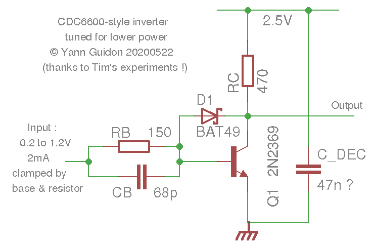
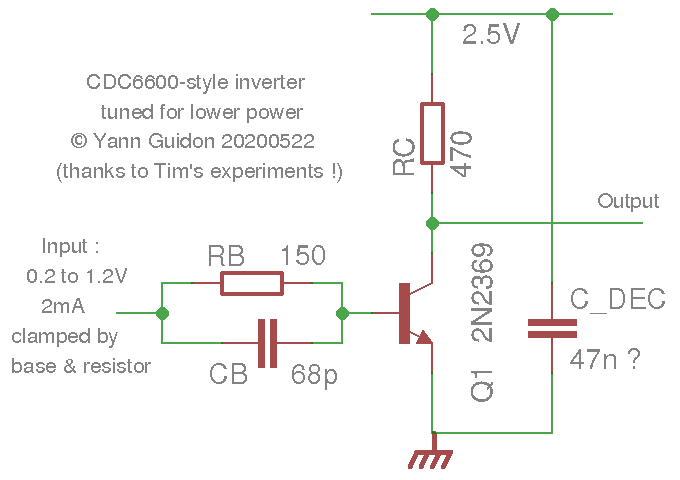
The new parameters are not far from the previous one :
Rb = 150 Ohms, Rc = 470 Ohms
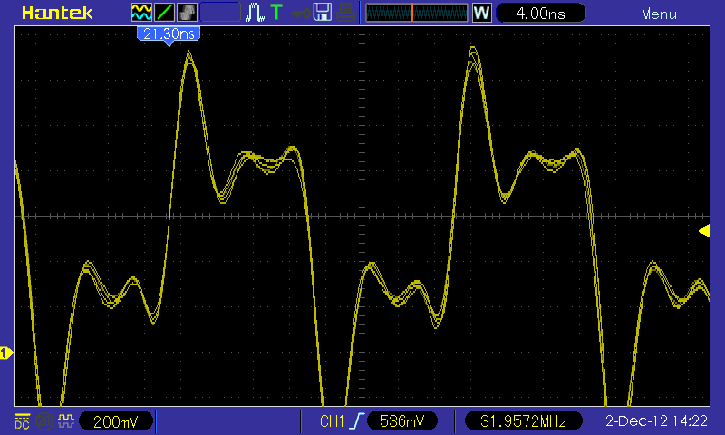
The change of Rb seems to have helped a bit : I now see the collector voltage saturated and not reaching Vcc (between 0.15 and 1.25V). Vb ranges from 0.18V to 0.9V => I'm now near the levels defined by CDC !
. Here is the waveform at the base : the 2N2369 is driven hard at 800mV ! Discharging it however seems to take some time...
The other change is the ample decoupling, 6×100nF + 3×10nF, I don't know if it helps but you're never too safe with that because later, I might unexpectedly scramble the local CB channels ;-)
Yet I don't see how/why I gained 30% speed with the same transistors (I replaced one by error) and almost the same resistors (ok the base resistor has lost 25% of its value... but it's worth it right ?)
Did I mistake a resistor somewhere ? Was one of the transistors "too slow" ? Is there a wrong resistor value in the first RingO ?
Something else is interesting : I'm now at 30mA but the last "record" was at held at 50mA so something serious is going on here ! Efficiency has jumped too !
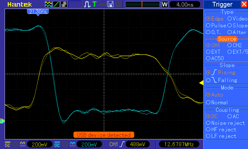
The signal falls in about 5ns on the 200MHz scope, which is close to the limits. There is some overshoot, very likely caused by the ground clip and the limited BW of the whole system.
Another good sign is that the falling edge (at the collector) is now the fast one, in 5ns :-) (we were puzzled that the rising edge was the fast one on the other board, might have been mistaken for the base ? nah...)
The rising edge takes about 12 ns to completely reach 1.1V and this will get only longer with more loading. But in 8ns, 1V is reached.
At 2.5V and 470 ohms shorted in DC to 0V, the collector current is drawing 5mA (approx.)
Add to this the other current source (the base capacitance and the transistor might have 10mA transients... So once again it's in line with the CDC specs :-)
The base current is defined by (Vc - Vb) / Rb = (1.2 - 0.85) / 150 => Ib = 2.3mA (at 2.5V, during DC ON) => in line with the expected values :-)
The circuit alternates between 5mA and 2.5mA, this averages to 3.7mA/9.3mW per inverter (FO1).
The delay :
This plot is from the base and collector of the same transistor, so we see the latency of the signal : about 5ns between the middle point of the rising edge on the base and the middle point of the falling edge of the collector. It takes about 8ns from the start of the base's rising edge to the end of the collector's falling edge...
The reverse however takes more time, due to RC loading.
set xlabel 'V'
set ylabel 'MHz'
set y2label 'mA'
set xr [1:4]
set yr [6:18]
set y2r [0:120]
set ytics 1
set y2tics 10
set key right bottom
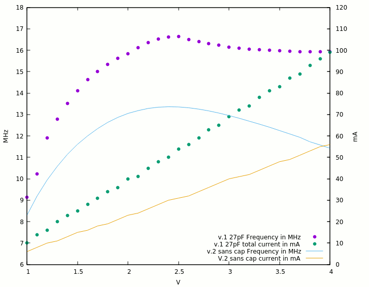
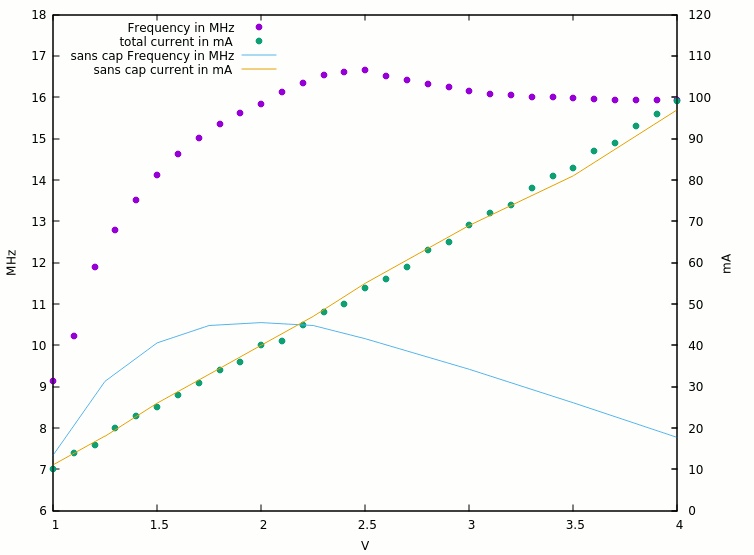
plot "27pf.dat" using 1:3 title "v.1 27pF Frequency in MHz" w points pt 7, \
"27pf.dat" using 1:2 axes x1y2 title "v.1 27pF total current in mA" w points pt 7, \
"ringo9_2_sans.txt" using 1:3 title "v.2 sans cap Frequency in MHz" w lines, \
"ringo9_2_sans.txt" using 1:2 axes x1y2 title "V.2 sans cap current in mA" w lines
The behaviour is temperature-sensitive...
The PSU's ammeter is really wiggly !
Efficiency at peak (2.5V) :
v1+27pf : 54mA 16.65MHz 135mW => 8.108mW/MHz
v2 : 31mA 13.354MHz 77.5mW => 5.8mW/MHz
Something really interesting is happening since v1 ! Is it thanks to all the decoupling ?
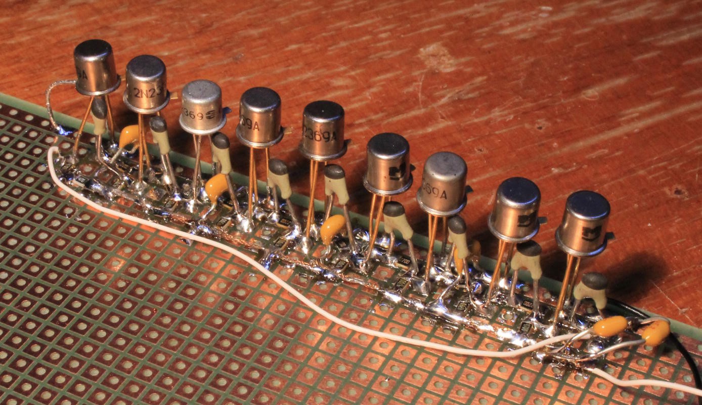
Ring oscillator with 9 levels of low-grade 2369 (according to their hFE).
Rb = 220, Rc = 470, like before.
1nF to decouple a pair of transistors.
But this time I add more capacitors : 100nF on the power input and 27pF to short each base resistor ! As usual, it's a step by step modification to help with understanding the effect of every change.
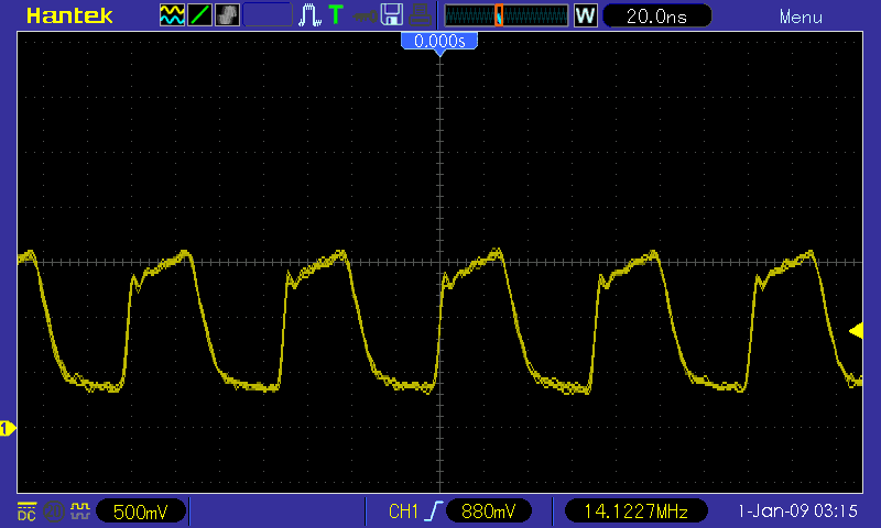
From the beginning, starting at about 10MHz, I saw the incremental increase of frequency : about 500KHz for each capacitor I added. I tested very often because I didn't want to spend any time spotting soldering error.
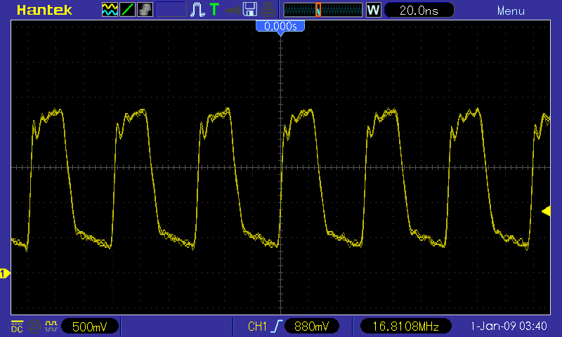
After a while I had the 9 capacitors wired and *bim* 16MHz without effort !
Some tuning later, a lot of blowing, and the best frequency I got was 16.8MHz !
That's at least 50% better than without the capacitors.
The power estimate is not very precise because the integrated ampere-meter has only so many digits... The delta column has some "noise" in it but this is useful anyway !
Gnuplotting gives nice results, sure !
Frequency vs voltage, Current vs voltage curve :
set xlabel 'V'
set ylabel 'MHz'
set y2label 'mA'
set xr [1:4]
set yr [6:18]
set y2r [0:120]
set ytics 1
set y2tics 10
set key left top
plot "27pf.dat" using 1:3 title "Frequency in MHz" w points pt 7,  \
     "27pf.dat" using 1:2 axes x1y2 title "total current in mA" w points pt 7,  \
     "sanscap.dat" using 1:3 title "sans cap Frequency in MHz" w lines, \
     "sanscap.dat" using 1:2 axes x1y2 title "sans cap current in mA" w lines
The increase is dramatic, yet the current has not noticeably changed.
The peak is clearly now around the 2.5V point.
Can you believe that even at 1.5V the system works nicely and faster than the previous version ?
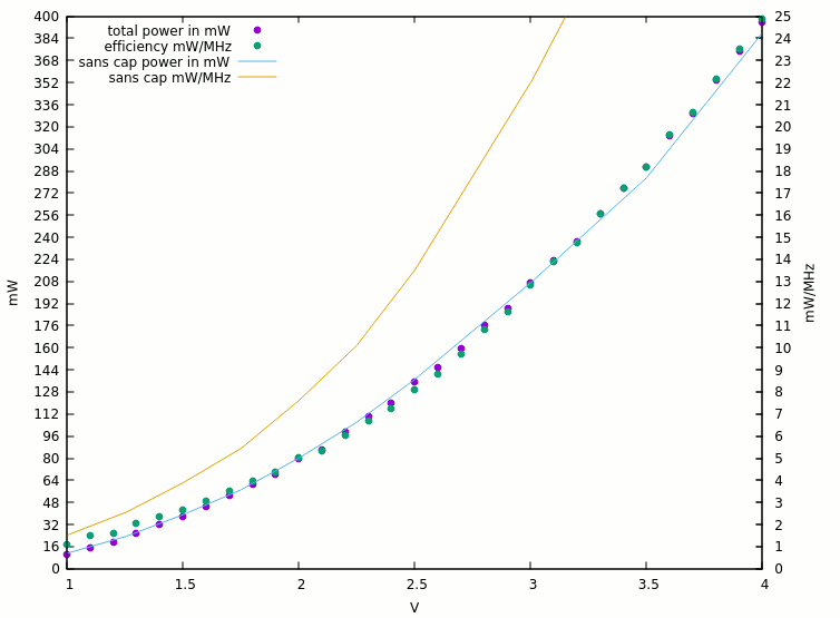
Efficiency curve :
set xlabel 'V'
set ylabel 'mW'
set y2label 'mW/MHz'
set xr [1:4]
set yr [0:400]
set y2r [0:25]
set ytics 16
set y2tics 1
set key left top
plot "27pf.dat"    using 1:4           title "total power in mW" w points pt 7,  \
     "27pf.dat"    using 1:5 axes x1y2 title "efficiency mW/MHz" w points pt 7, \
     "sanscap.dat" using 1:4           title "sans cap power in mW" w lines, \
     "sanscap.dat" using 1:5 axes x1y2 title "sans cap mW/MHz"      w lines
The power curve is very very close but the efficiency is clearly better.
Low voltage RTL FTW !
We'll see if/how more capacitance helps ...
Efficiency slope:
setkeyleft top
plot "27pf.dat"using1:6 title "efficiency slope (mW/V/10)" w points pt 7
Not surprising : with a quadratic curve, the slop increases linerarly... but the Vbe effect is felt between 1.5 and 2V.
It's noisy (due to current measurement imprecision) but it's easy to guess that the lower values are more interesting ;-)
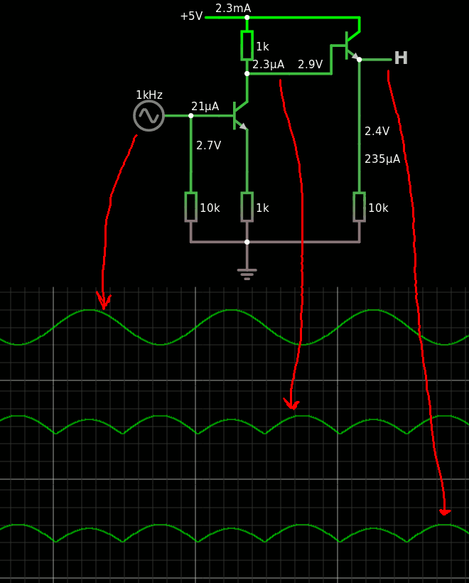
So I was Falstad'ing some ECL/differential amplifier topologies and playing with the resistor values ratios...
I found some strange behaviours with this single-ended circuit when the collector and emitter resistors are equal.
At 5V the turning point is at 3.1V, so I created a sine wave centered around 3V with +/- 1V peaks. The output looks like a rectified version...
The effect disappears when the ratio of the resistors is modified. This might be a desired effect or an unwanted behaviour, and since I'm playing with ECL topologies, I want to avoid this so I need to understand what is going on.
This is important because I would like to save a transistor at the common emitter node so the resistor value must be well chosen. It's good to know that a 1/1 ratio is BAD, and changing it affects the kink point...
But OTOH it opens up potential for fun, such as sound effects :-P
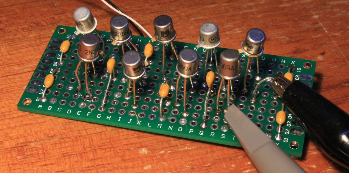
With a sporadic and limited access to the workshop (at last !) I can finally try new ideas ! I have meanwhile received 9K PMBT2369 in SMD but I decided to use the old stock of 50pc 2N2369A in metal can, that was waiting in a small bag that I received from various sources... What can be closer to the CDC era ? (A motor-generator ? :-P)
This is a "mixed bag" with at least 2 sources or makers, some with golden legs, and I decided to test them. Just because I now have a better tester and it's good to see if/how the different types differ...
Most "golden" parts fall in the lower bins and the tinned ones have overall the best gain. I made 3 bins :
< 60 (lowest is 46)
< 84
higher (a few up to 114 and one at 119)
and then I use the lower gain ones to build the RingO, with 9 parts to give a low-enough frequency that makes 'scoping reasonable.
I could have made a > 100 bin but
I just wanted to have a look at the spec spread
I wanted to weed out the lemons (and use them first to establish a baseline)
Rb = 220 (that's what I have in stock right now, close enough)
Afterthought : I should have tried 100 Ohms for Rb. Or even 47/50 ohms maybe....
After-afterthought : or 330 ohms (see near the end)
And the soldering iron was turned on !
For the sake of simplicity I omitted the caps. They used too much room. Next time I'll look at the SMD stock.
I added 1nF to decouple every pair of transistor (that's 5nF but spread to ease HF transients)
I found some partial reels of SMD Schottky diodes but once again, decided to not use them yet.
So I wanted to establish a baseline for speed and more importantly : explore the power vs speed envelope because... Tim found that a LOT of power was wasted. I would like to get a gate that is still "pretty fast" and yet consumes at least 10 times less power.
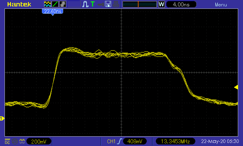
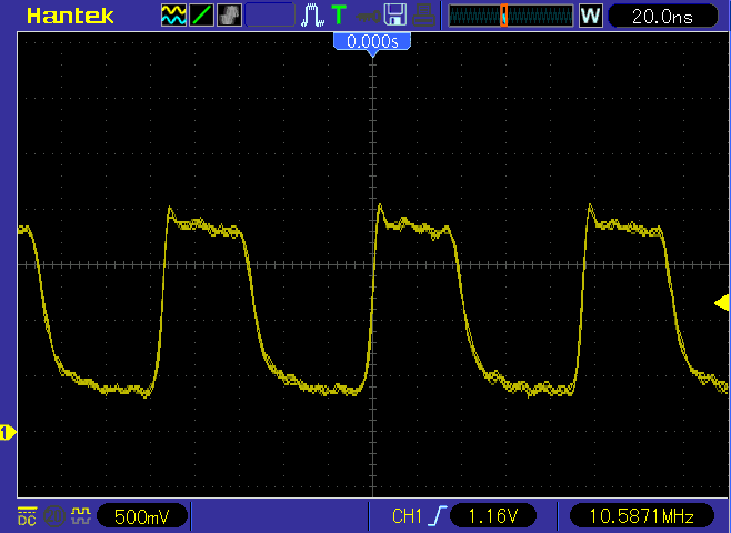
For the measurements I used a 200MHz digital scope with 10x probe. The output waveform is pretty nice and quite square-y :-) No funky feature is noticed, it's plain old RTL and I didn't bother to measure the rise/fall time because the measurement circuit is not optimised.
Still it's very telling.
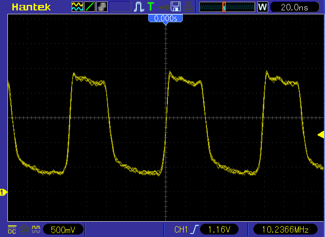
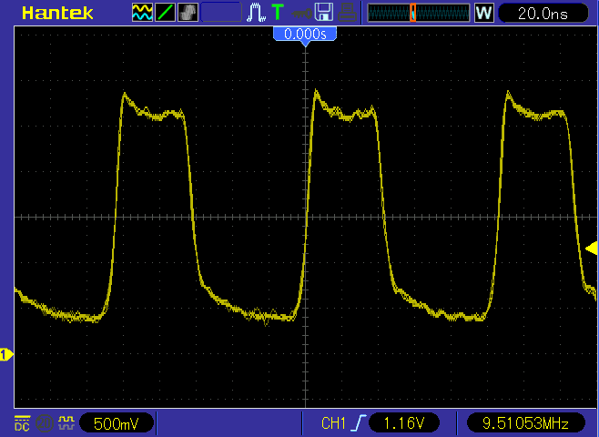
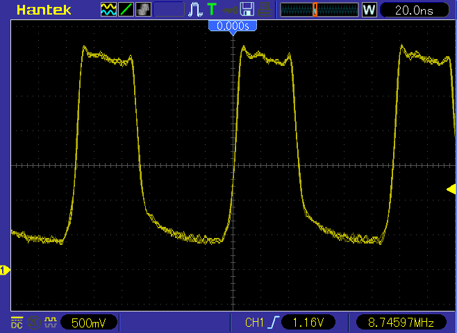
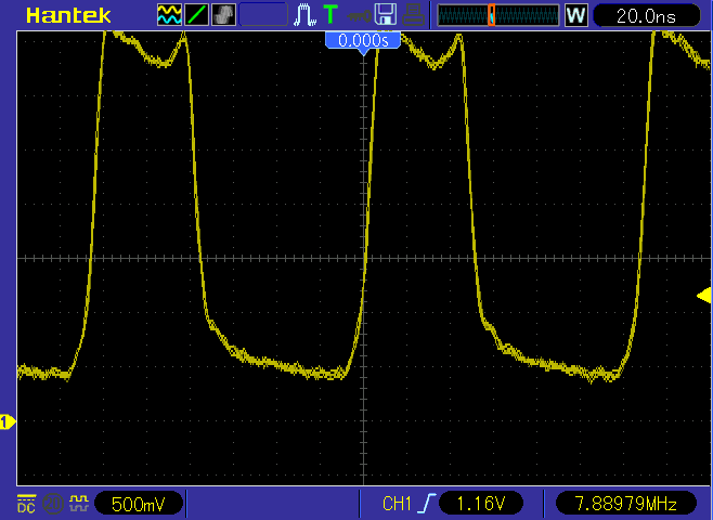
2V:
2.5V:
3V:
3.5V:
4V:
4.5V:
5V:
Rise time is about 5ns. Which is odd since I expected that RC would dominate it.
In fact something else is happening : it seems that the transistor has a harder work to totally saturate and keep Vce sat to a sufficiently low value. This in turn reduces the frequency because the transistor turns off later.
At 5V the circuit doesn't seem to get hot, maybe thanks to the help of the metal cans and the resistors directly soldered to thick metal that can spread the heat.
You can find a curve that is similar to what Tim found already :
Vcc Total Freq.
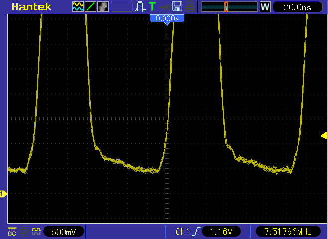
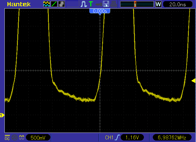
5V 123mA 6.98MHz <= never mind.
4.5V 109 7.37
4V 97 7.77
3.5V 81 8.61
3V 69 9.42 <= why waste so much power ?
2.5V 55 10.16
2.25 47 10.48
2V 40 10.55 <= sweet spot !
1.75 33 10.48
1.5V 26 10.06
1.25 18 9.13
1V 11 7.34 <= wow, that's still good :-D
The frequency is measured by the scope but not finely calibrated. My HP freqmeter wouldn't accept the raw signal, something to do with ringing and probe impedance, I'll check that later. Still you can find the important features.
With my choice of parts, I find that the sweet spot is in the 1.75V-2.25V range, as roughly expected, so I'm pretty happy ! But there is more to that curve.
The power/speed ratio decreases faster than the voltage ! (due to the Vbe effect and the RI² factor)
Going from 3Vcc to 2Vcc gives you almost 3x power advantage for 10% speed gain... And over the "sweet spot" frequency range (1.75-2.25V), the power (almost) doubles !
At 2Vcc, each transistor draws less than 1mW and is at its fastest point, using a very simple circuit. If you consider a 3-input gate with all the inputs on, the current is shared among the 3 transistors so it can go lower but then, the power from all the base currents becomes prevalent.
Aparte:
If you consider the reliability considerations of the CDC6600, drawing less power would have been very easy and the inherent costs (power supply, cooling etc.) are insane. See the Living Computer Museum video where they explain that the chilling water tower and the piping cost them much more than the rest ! And heat management was a defining trait of these machines. So it's good to have the numbers to vindicate my quest to reduce the supply voltage.
So what convinced Seymour Cray to burn so much power and explode the budgets ?
Edit: It seems the answer is in fig.17 of p.26 of the "Thornton book" : "buy" as much current as they can so the rise time of the transistor would be negligible compared to the RC load of the node. Furthermore the power supply is not capacitor-filtered but direct from tri-400Hz which has a 2400Hz ripple so they needed that margin too... I suppose they studied the capacitor method but the load's RC might have been a dominant speed limiter. This is a cautionary tale for the results of RingO circuits : they don't directly apply to real circuits.
Something else is interesting, I had to share it ;-)
This circuit tests the basic inverter but you can't make a computer with this. The minimal theoretical fanout is 2, 3 becomes almost practical, VLSI CMOS chips target 4, and you need at least 5 or more to make anything interesting. Yet a majority of the practical cases are 2 or 3... But the higher, the better !!!
The CDC6600 has some interesting "rules of thumb" concerning fanout:
FO=5 for intra-module circuits
FO=2 for inter-module transmission
Not more than 6 collectors tied together
(see p.25 of the Thornton book) and I'd like to check if they still apply here.
The first thing is to reduce the pull-up resistor as the number of gates increases. Page 25 tells that CDC adjusts it, as well as Rb. Let's compare the values of Rc (called RL) with the E12 series :-)
But for a good fanout, the precision (or exact match) of the pull-up is not critical. Two things are, though :
Drive the base hard enough to lower the output well enough. CDC specifies < 0.2V, which occurs at Ib=1mA (see: the Thornton book, p.22) => the gain is low at the highest frequencies so the base current increases during transients, up to 3mA (see below)
Pump enough current through the collector while remaining within the limits of power dissipation : while conducting, ideally, the transistor dissipates (Ib*Vbe)+(Ic*Vce)=0.7+2mW=2.7mW in the best, continuous case (supposing 10mA in the collector). In practice, the transients add more current here and there.... but this is compensated by the "off" states. Here we already see that in average, a transistor shouldn't dissipate more than 1.5mW in average. RL burns the majority of the total power, all the time !
The gain would directly dictate the fanout : at Ib=1mA and Ic=10mA we would expect a fanout of 10 but it's not working like that. First, the base current would increase even higher (during transients) and the base current is not directly driven by the driving transistor, which actually short-circuits it. The collector swings from 0 to 1.2V, or 0% to 20% of 6Vcc, Ib would receive about 80% of Ic. The fanout would be in the range of 3 to 4 (not counting PCB parasitics)
By the way, the "Thornton book" ("Design of a computer : the Control Data 6600") makes more sense now, and I can better read between the lines of several paragraphs that were cryptic. I had forgotten that the "diode equivalent" of Vbe should limit the value of the input voltage and the Rb must be lower than the 220 I chose before.
If Vin=1.2V, with Vbe=0.7V, then Urb = 1.2-0.7= 0.5V : the base resistor drops half a Volt, which is not the case in my prototype (and probably not @Tim's ?) but it's easy to estimate the value : Ib=1mA, Urb=0.5 so Rb=Urb/Ib=500 ohms (wait, what ? that's not consistent with my estimates by a factor of 10 ! And the CDC6600 has Rb about 150 ohms so why is it different ? Poor transient gain ?)
TODO : measure the base resistor drop. I 'scoped the traces above at the collector node but I didn't trace the base voltage (though it's expected to wiggle around 0.7V) and it seems the base resistor voltage is much higher, since the collector can rise up to Vcc (must be re-checked !) despite the lower value : 220 < 500 as calculated in the previous paragraph. Something is not right and I'll have to retry with 47 ohms. Or even a trimpot.
Base-collector "Baker clamps" are cool but as Tim noted, they reduce the margin.
However, 2 silicon diodes in series (between the ground/emitter and the collector) would drop about 1.4V, which is about right for the CDC logic levels. That would be only 2 diodes per gate output with a higher tolerance than the Schottky clamp diodes, it would preserve the noise margin and the base current would be easily controlled by the base resistor.
The problem would be speed again because silicon diodes exhibit a non-negligible capacitance... PMBT2369 is rated at 4pF max while the planar 1N4148 is also rated at 4pF and 4ns (whatever this actually means and whether it applies).
EDIT: BA243 is 1.5pF and capacitors in series have lower equivalent capacitance. Furthermore the diode would not switch from reverse to forward bias, which avoids a trouble-making behaviour (unless your name is @Ted Yapo and you want to build a Diode Clock) but it would work as a sort of Zener and go from 0V to 1.2V
Another consideration : The PMBT2369 datasheet shows hFE minimum of 20. Gain should be considered "low" during transients and many measurements are under the condition "Ic = 10 mA; Ic = 1 mA" (actual gain=10) and the base current reaches 3mA for the rise time measurement (and -1.5mA for falling time). The tripled current would explain why practical circuits have such a low base resistor...
More considerations in the comments section :-)
... and more apologies for editing this log so many times ;-)
PS: Great find, Tim, you didn't say it loud enough though ;-)
Found in cross-reference chapter of Fairchild's 1985 "Discrete Data Book"
 Yann Guidon / YGDES