Yann Guidon / YGDES
-
Why is ECL faster ?
07/12/2018 at 11:25 • 9 commentsLately I was looking for very fast diodes to design faster DTL/TTL discrete gates.
- silicon epitaxial diodes can be quite fast but still have a limited frequency of rectification (particularly the cheap ones).
- As noted by @K.C. Lee on #YGREC-ECL : "Carrier mobility isn't as good as electrons. That's why NPN, N-MOSFET
have better performance than their PNP, P-MOSFET counterparts." so a complementary TTL gates, with a PNP input stage, would probably be speed-limited by the input transistors.
@Al Williams just released an article on had.com :
The recovery time makes a difference in several designs including switching power supplies. If you dig into the physics, there is a usually a trade-off between several other parameters and recovery time. Just to give you an idea, the datasheet for a BAT42 Schottky diode says the reverse recovery time at 10mA is no more than 5 ns."
I don't know the exact figures in practice in a logic gate but 5ns of recovery is not good. That's about the propagation time of a DCTL inverter in the CDC6600.
Rectification speed was already a burning subject in the 40s because it was essential to the war effort (faster diodes means higher carrier frequencies, shorter wavelengths and better radar resolution)
ECL prevents all these issues because
- there are only NPN transistors
- no diode (no recovery time)
- no saturation
However there are more transistors... so maybe DCTL is an interesting alternative ?
-
Interactive Simulations of DEC R-Series Logic
07/04/2018 at 23:15 • 3 commentsFor those interested in visualising the operation of DEC R-Series Logic, I have created these two short animations which simulate the operation of an Inverter and a Complementing Flip-Flop:
Inverter:
https://cdn.hackaday.io/files/8449361482016/DEC%20R-Series%20Logic%20Inverter.mp4
Flip-Flop:
https://cdn.hackaday.io/files/8449361482016/DEC%20R-Series%20Logic%20Flip%20Flop.mp4
You can find the schematic files for these simulations saved here:
https://cdn.hackaday.io/files/8449361482016/DEC%20R-Series%20Logic%20Inverter.txthttps://cdn.hackaday.io/files/8449361482016/DEC%20R-Series%20Logic%20Flip%20Flop.txt
-
Direct Coupled Transistor Logic
06/22/2018 at 04:22 • 13 commentsIntroduction
@Yann Guidon / YGDESasked me to do a write-up of the Direct Coupled Transistor Logic (DCTL) of the famous CDC 6600 computer. When it was released, and for some years, the CDC 6600 was one of the fastest and most powerful computers in the world. When we take a look at the logic family that it used, it will be obvious to see why:
- It uses very few components, primarily transistors, with no diodes
- The transistors which perform the logic are driven very hard, to the point where the quality of the transistor fabrication actually matters a great deal
- The logic levels are dangerously close together (in the 6600’s case “0” = 0.2V, and “1” = 1.2V).
- The cacading and interlinked circuits must be carefully “tuned” input and output impedances MUST agree precisely, or the logic will not function due to noise or otherwise.
The Basic Unit: The Inverter
There are primarily two main articles available online which deal with the electronic description of DCTL logic:
and
James B. Angell, “Direct-Coupled Logic Circuitry” (1958) Proceedings of the Western Joint Computer Conference: Contrasts in Computers, 22-27. https://www.computer.org/csdl/proceedings/afips/1958/5052/00/50520022.pdf
This is not a great deal. On Bitsavers, there is no folder for the engineering documents of the 6600, as opposed to the 1406, and 3600-series CDC logic, which I also aim to cover because it is a very interesting high-speed DTL.
So bear in mind that the information I am presenting here is limited, and if you want to build your own DCTL circuits you are most likely going to have to design your own, because there are no complete design documents online for the 6600 which you would have been able to copy and modify.
Anyway here is the basic building block of DCTL:
The CDC 6600’s inverter:
![]()
The 1950s DCTL inverter:
![]()
By the time the 6600 was built, transistor fabrication had developed and improved markedly. In fact the first few pages of the chapter of the CDC-published book on the digital electronics of the 6600’s DCTL go on about how the new silicon transistors they used in ‘69/‘70 made the 6600 possible. So this explains why the 6600 uses NPNs, as opposed to the older implementation using PNPs.
As you can see, you would be forgiven for mistaking DCTL with Resistor-Transistor Logic (RTL) if you had only an inverter to look at. I agree with the speculation on the (tiny) Wikipedia article on DCTL that it evolved from RTL.
Obviously the thought process that lead to developing this logic family was “what if we had RTL but got rid of all the resistors?” The point of having resistors in RTL is to allow you to increase the voltage margins of the logic levels. It also allows you to better control the flow of current throughout the circuitry and match the impedances of the inputs and outputs.
The first problem you have with DCTL is – how do you make sure you can switch transistors without driving them too far into saturation? The solution is to use transistors with special impedances and gain ratios.
Take a look at the special transistor characteristics that the conference proceeding document outlines:
![]()
This is obviously based on an old understanding of exactly how well-designed transistors are, but you can see we’re only switching very small amounts of current, and the V(BE) of the operation of the transistors when in saturation/conduction is far lower than your standard BC548/9 or 2N3904/6.
I haven’t checked yet, but I believe transistors with these kinds of characteristics should be able to be obtained cheaply. The maximum switching time required in this specification from the 1950s is easily obtained with modern discrete transistors.
DCTL Logic Levels
The logic levels of DCTL circuitry in the 6600 are very very close together. As you can see the V(BE) of the 6600 transistors closer resembles the operation of modern transistors.
![]()
At this stage, I became very interested about how noise is dealt with in DCTL circuits, because the logic levels are nowhere near as far apart as 0-5V as in TTL.
Angell in the conference proceeding explains how it is possible to minimise noise in DCTL:
Some kinds of noise are comparatively unimportant in DCTL whereas others are potentially severe. Because of the very low impedance level of “on” circuits, capacitive pickup is generally negligible. Power-supply fluctuations are usually unimportant, because voltage translation circuits are not required and the majority of a complete logical system can, if desired, be run from a single supply. On the other hand, because of the small voltage swings which are experienced in DCTL, inductive coupling in either multiconductor cable or via ground leads may be troublesome.
It is generally felt that with germanium transistors a maximum induced noise or the order of 25 millivolts can be tolerated; this figure amounts to 10% of the normally encountered voltage swings.The article then goes on to detail how it is possible to reduce noise. Please see the article for more.
Matching Impedances
The whole gambit of designing DCTL circuits depends on making sure different logic elements have impedances which agree. Because of the low conducting collector-to-emitter voltages in DCTL, the transistors involved in this logic family will have quite low gain. The game you play with you tangle with DCTL is attempting to have as much gain as possible to increase fan-out.
Generally speaking, fan-in will be much higher than fan-out in this logic family.
To take a look at the limits you come up against when designing DCTL circuits, consider the following interchange:
![]()
This interchange is n paralleled OR gates driving m paralleled loads.
Angell explains that two conditions are necessary in order to make this interchange work:
- When all the input gates are off (V( C)=0.2V), all the output loads must be on (V( C)=1.2V).
- The conduction in any one of the OR gates must turn off all the output loads.
The first condition is fulfilled by the following inequality:
![]()
The term on the left is the smallest possible load current. The term on the right is the leakage current in all of the gates in the interchange plus the minimum required load.
The second condition is satisfied by the following inequality:
![]()
It means that the collector current of one conducting gate must be greater than the maximum possible current in the load resistor. Here, the node voltage is equal to the specific limit voltage required to maintain the load transistors in the nonconducting state.
So this gives you the limits within which you can match the impedance of the inputs and outputs of the interchange. This will help you determine the fan-in and fan-out, and set the load resistor value.
The important factors in this particular example, therefore, are:
- The input impedance of a conducting transistor must not be too low. This problem can be solved by setting a maximum limit on the the ON base current for a particular base voltage. This way, no one output transistor will take too much of the available driving current.
- The output impedance of the OR transistor network must not be too high. One method of solving this problem is to make sure that the V(CE) of the input transistors is LESS than a certain limit for a given I( C) and V(BE). Another method would be to limit the I( C) with respect to given V(BE) and V(CE). The absolute minimum limit for either of these conditions, the lowest V(CE) or lowest I( C) is determined by the minimum transistor gain. This minimum individual transistor gain will be much greater than the overall circuit gain. However, this individual transistor gain will be much smaller than if the transistor were in the active or non-saturated region. So it is a careful balancing act of switching current from the collectors of input OR network into the bases of the output network.
- The “off” collecor current of a non-conducting transistor must not be too large. This means the “off” I( C) must have a maximum limit compared to its “off”, non-conducting base voltage (V(BE)).
All of this boils down to the following: In order to have compatible connections between DCTL logical elements, V(CE) “on” [Logical “0”] =< V(BE) “off” [Logical “1”] for any particular logical element. Angell explains that it is permissible to sacrifice gain in some instances in order to reduce the V(CE) of a given logic element.
Combining the two inequalities above when considering the above interchange, you can solve for the gain of an individual transistor in conduction. This produces the following inequality:
![]()
As Angell explains, the result shows that the input transistor gain must be greater than the (a) circuit gain; multiplied by (b) m, the number of output loads; and ( c) factors accounting for the tolerances of the components.
You can derive a rule of thumb to follow if the networks of logic elements is too great:
I( C) “on” / I(B) “on” [Logical “0”] > 2m
So the gain of a saturated transistor must be greater than twice the number of output loads.
CDC 6600 Rules of Thumb
The general rules CDC outlines for 6600 DCTL is:
- One transistor collector can drive five bases within a module
- One collector can drive two local bases within a module and two bases by back-panel twisted par on one other module
- Six collectors can be connected within a module
Selected Common Logic Elements
There is therefore a lot of work required to match logic element input and output impedances. But, the advantage to all this work is that DCTL logic elements are actually very simple.
Consider the following 6600 NPN and 1950s PNP basic logic elements:
![]()
![]()
![]()
After matching all of the impedances of logic elements, you are rewarded with very simple circuitry.
![]()
![]()
Switching Times
One can assume that this circuitry switches and propagates faster than the famous and standard hobbyist DTL. I do not have exact measurements, however the CDC documentation assumes the propagation delay of an inverter is 5 nanoseconds.
Conclusion
Although fairly fiddly, this seems like an interesting logic family.
I will cover CDC’s 1604 and 3600 DTL logic in the next write-up.
-
TTL inside
06/22/2018 at 02:49 • 5 commentsRecently Steve Toner showed his sticker "TTL inside":
https://hackaday.io/project/27392-stupid-computer/log/147982-logo
![]()
So I decided to order my own version of that (in RED):
![]()
After applying to the plastic box, which could be used for my future TTL computer, it looks like this:
![]()
Thanks, Steve Toner! ;)
P.S. For some reason they don't have proper capital letters for TTL in both cases, but anyway it looks awesome :)
P.P.S. Interesting thing - another "whatever inside" vendor actually does have capital letters - see my personal G4 laptop for example ;)
![]()
It's a different font, but still. Unfortunately they disappeared from eBay some time ago :(
-
ECL or CTL : what's the fastest topology for discrete gates ? [updated]
06/14/2018 at 06:44 • 20 commentsEDIT 20180918 : Please see the erratum/confession at the bottom !
Private discussions and readings (books, online etc.) bring a very important question : what's the fastest gate for discrete circuits ?
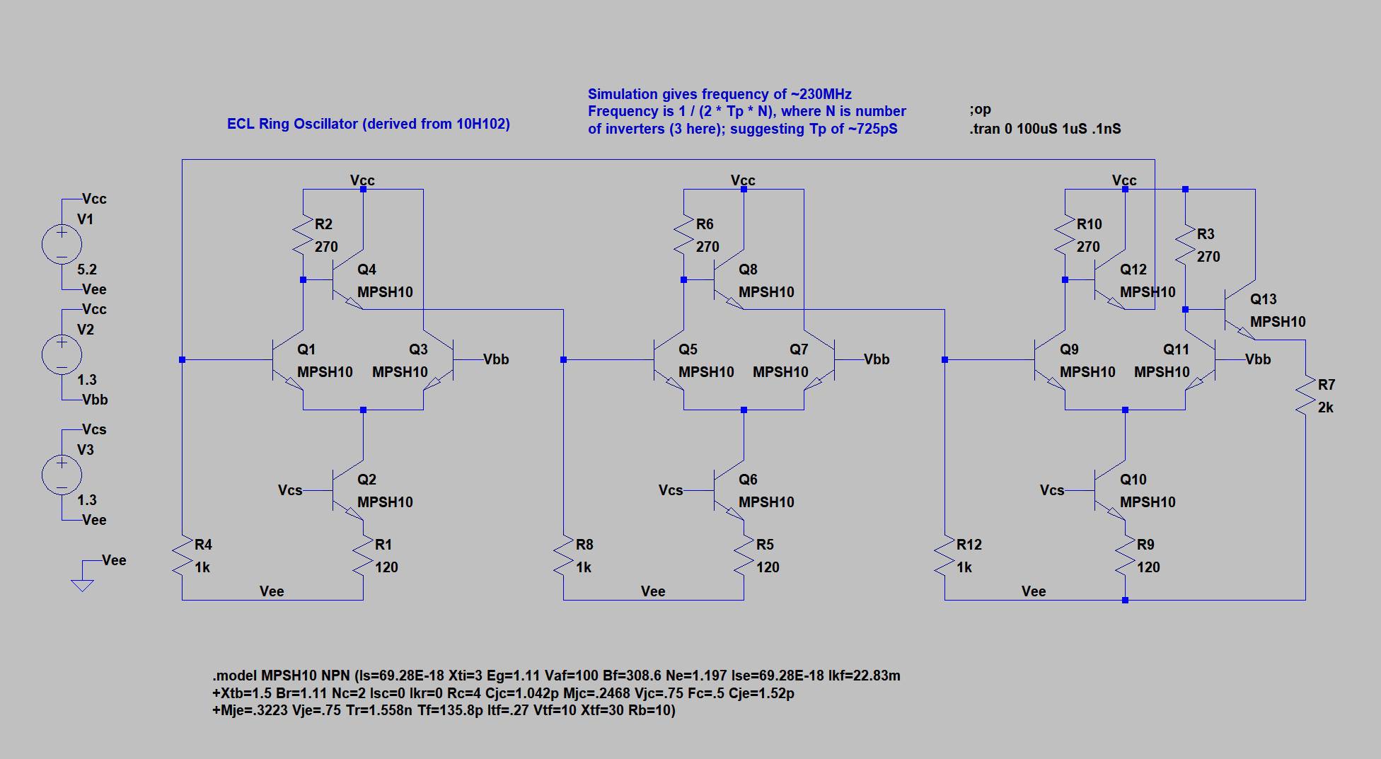
ECL is notoriously fast. @Dana Myersrecently played with it and reached about 0,5ns propagation time in inverters in a ring oscillator, on a breadboard and with a fistful of MPSH10.
https://www.facebook.com/groups/1233645553343772/permalink/2057225387652447/
![]()
(note : the ideal current is about 4mA per gate and the oscillator reaches 307MHz on breadboard)
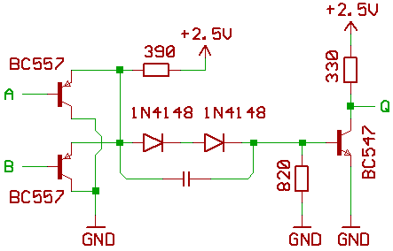
On the other hand, Complementary Transistor Logic is a bit like DTL but the input diode is replaced by a PNP. This greatly increases the input impedance and helps with many things. Operating voltage and current might be significantly lower, it even reduces the transistors count by 2 compared to ECL. But if it's easy to get one sort of FAST transistors, the complementary type might not be easy, as cheap or as fast... I have only stocked one type of germanium (PNP, because Ge NPN is rare) and silicon (well, I have mostly NPN, some PNP but i have no idea how to find a PNP equivalent of BFS480...
![]()
(as usual, the 2 diodes in series could be replaced by a red LED ?)
The BC857 has a high gain so the input current can be very low and this reduces fanin/fanout issues. The speedup capacitor might need some tuning, maybe 1 or 2nF ? And the resistors could be reduced to increase current and speed.
I've also read mentions of hysteresis of CTL gates, due maybe to capacitance, which can reduce the operating speed. A Schottky diode might be needed to remove bias buildup... or even add a resistor in parallel with the speedup capacitor ? Or what about simply avoiding the voltage shift by using more power rails ?
Another parameter is : sometimes, using better and faster transistors simply lets the gate run faster. But it can come at a high price so topology is still critical...
Now, the only way to compare is to try, right ?
![]()
(repost courtesy of @Dana Myers )
Just for the sake of discussion, Fairchild had their own TTL family back in the day when the 74-series was not an industry standard (or Fairchild had their "74F" series). They did TR, TD and TT : transistor-resistor logic, transistor-diode logic and here transistor-transistor logic. The datasheet shows no Baker clamp, but R5 might have helped...![]()
But 5 transistors for one NAND, that's similar to ECL density :-D
EDIT 20180918 : Mea Culpa !
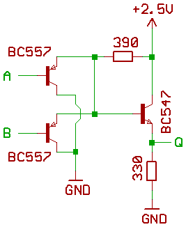
Apparently I made a big mistake and used the wrong schematic for CTL.
CTL seems to be derived from ECL and is claimed to be even faster (for certain values of "fast" because I still have to try it)From what I have gathered from the MT15 project, with BC847\BC857:
- TTL with some load: 50ns.
- TTL Schottky clamped: 35ns.
- Differential ECL: 20ns.
- CTL two input AND gate: maybe 5ns. To be measured...
The schematic is subtly different from the one I included earlier :
![]()
As above, the inputs are PNPs that short the base node to GND. However the difference with the previous schematic is the output stage: it is a follower and not a "shorter to GND", so it does not saturate.
Note also that the gate above is a AND gate and no inversion takes place. I'd love to see an inverter, a MUX, a OR, a XOR...
I'm also unsure about the logic levels, temperature susceptibility and noise : I'll have to compare to ECL and DCTL :-P
The availability of a richer set of logic functions is critical for me, but there is an added simplicity to CTL : one can use SIL resistor networks to keep the parts count low and share a single package for several gates. No caps, no diodes, only 2 resistors with very close values...
-
The Electronics of IBM Standard Modular System Logic
03/27/2018 at 06:07 • 9 commentsIntroduction
Okay! We’ve had a look at the Diode-Transistor Logic of the DEC R-Series Logic, but that isn’t the only electronic logic system that was employed in building discrete discrete component computers. As I explained in the post on R-Series logic, back in 2013 it was some IBM computer which implemented an exotic electronic logic system which lead me to go down the “popular” DTL path. I will continue my investigation into different logic systems in this post with the IBM Standard Modular System (SMS) logic. IBM SMS logic doesn’t just implement specific systems of logic families, but also whole different logic families! The IBM SMS uses what is now known as Emitter-Coupled Logic (ECL), as well at Resistor-Transistor (RTL) logic and DTL. ECL is a very difficult logic family, and RTL is unpopular in hacker circles, so we will look at the IBM SMS DTL logic implementation first, and then just look at their ECL circuits. The Don Lancaster RTL Cookbook is sufficient really for people who wish to build discrete component RTL computers.
IBM Standard Modular System Diode-Transistor Logic
I have obtained the electronic description of the different IBM logic implementations from the IBM Transistor Component Circuits volume of the Customer Engineering Manual of Instruction. You can find this manual easily by searching the above words on the internet. There are also manuals describing the exact electronic schematics of the flip-chip cards used in IBM mainframes such as the 7070 and the 7090. They’re worth a look if you want some inspiration for solving a particular concrete problem.
Logic Levels
The SMS DTL system uses four different logic levels. They are divided into two fundamental kinds, “T” line levels and “U” line levels.
![The IBM SMS DTL Logic Levels]()
As you can see, positive T levels swing from -0.7V to 6.0V, whereas negative T levels swing from 1.4V to -6.0V. Positive U levels go from 0V to -7.4V, and negative U levels move from -5.3V to -12V. There are schematics in the Transistor Component Circuits manual for how to convert T and U lines to each other. They’re not worth mentioning here because we don’t need to get into that much detail.
The Fundamental Gates
Below you can find the schematic for the fundamental positive-logic NAND gate, or negative-logic NOR gate. IBM doesn’t use the standard terminology for these gates, probably because the manuals for this system were written in the late-50s early-60s, before the terminology settled to what we know today. You’ll also notice that the symbols for transistors here are also non-standard by contemporary wisdom. The same reason should apply here. We won’t concern ourselves here with the physical electronic characteristics of the transistors and the diodes. I’ll put some work into that later.
![The IBM SMS DTL Basic Gates]()
There are three gates specified here. As you can see:
- It is possible to interface the output of a DTL gate into ECL gates.
- The first gate (at the top) takes a +U logic level and outputs a -T logic level.
- The second gate (Gate “A”) takes a +U input and outputs a +T logic level.
- The third gate (Gate “B”) is similar to the first one: it recieves a +U level, and outputs a -T level, as well as being able to interface with ECL gates.
It is possible to take T-line inputs and output U-line logic:
![The IBM SMS DTL U-line Output]()
These gates can drive ECL gates as well! Note well that the T-line inputs for the above gates are NEGATIVE T line levels (-T levels).
There are other inverters specified in this manual, such as “Power Inverters”, which drive bigger loads and have bigger gate fan-outs. You can peruse the manual to look at those at your leisure.
There are also emitter-follower gates, which amplify the current of signals. There are also circuits for driving indicators connected to T and U line signals.
Basic Flip-Flops
Below you can find the schematic for a basic IBM SMS flip-flop:
![IBM SMS Flip-Flop]()
This complex flip-flop can be set with what IBM describe as “AC signals” and “DC signals”. I assume they mean changing digital signals for “AC” and static current signals for “DC”.
It also outputs U and T level signals. The emitter-follower outputs at the bottom are T-level, and the inverter outputs at the top are U level. If I am right, there are both the POSITIVE versions of these signals.
Miscellaneous
There are a great deal of other gates specified in this manual which may interest the reader. They are debouncers, oscillators, more logic level converters, and so on. Check out the manual for a better look.
IBM Standard Modular System Emitter-Coupled Logic
Logic Levels
Below you can find the definition of the four different forms of logic levels that IBM’s SMS ECL uses:
![IBM SMS ECL Logic Levels]()
The Positive and Negative P and N levels are fairly reminiscent of the T and U lines of IBM SMS DTL. As you will see as we look at the basic gates of SMS ECL, the actual voltages that the gates use will be much much closer together than in SMS DTL. This is because electrical current is the bearer of logic meaning in ECL. The whole point of ECL gates is to very quickly switch electrical current with transistors that are NOT saturated or cut off. This makes ECL a much faster logic family to use, but it also means ECL uses a great deal more power, because ECL systems typically have large amounts of current flowing through them. The greater the current, the higher the amount of power the system ends up using.
Fundamental Gates
Below please find two schematics for the fundamental Positive AND and Negative OR gate:
![Positive AND, Negative OR, ECL]()
and Negative AND and Positive gate:
![Neg AND, Pos OR, ECL]()
They respectively take N and P inputs, and output both in-phase and out-of-phase opposite fundamental logic level outputs. That is, if you feed the first gate, the Positive AND gate, an N level signal, it will output a P level signal of both phases: +P and -P. The opposite goes for the Negative AND: a P input and an N output.
There are other circuits specified in the manual - Emitter followers, for driving large numbers of gates, and Power Inverters, which convert ECL logic into DTL logic.
I am actually amazed about how it is possible to combine different logic families together into one computer. It just goes to show that if you have a lot of time, energy and resources, you can construct incredibly eclectic systems.
Here is the schematic for an N-level ECL to U-level DTL converter, for instance:
![ECL to DTL converter]()
There are also line drivers, transmission drivers, indicator drivers, and more in this manual.
Basic Flip-Flops
IBM SMS ECL flip-flops are incredibly complex. In fact I think they may be of absolutely no use whatsoever to the ordinary hacker - they require many capacitors and inductors. See below:
![ECL Flip-Flop]()
The flip-flop does also not receive or output DC signals. It is a purely AC operated gate. I now revise what I took “AC signal” to mean - it is an entirely analogue current signal. Perhaps this is incorrect, but as you can see below, basic flip-flops made from AND and OR gates are called “DC triggers”:
![Basic ECL Flip-Flop]()
As the schematic shows, you need to delay input signals to make sure you don’t create racing conditions, which would cause the flip-flop to enter a state of feedback.
Conclusion
Hopefully someone finds this useful! As always, for more information, see my blog http://bootlicker.party/
-
Bizarre DTL Logic Levels - The Discrete Component PDP-8
03/26/2018 at 05:04 • 6 commentsIntroduction
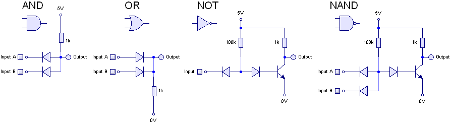
Hello! This is Blair Vidakovich. I was recently given entry into the hackaday TTLers group! I have tried many times, unsuccessfully, to create a discrete component computer. My basic logic element was a NAND gate, and I was using a popular form of DTL logic unit. I was copying the same electronic schematic as the Tiny Tim DTL computer. You can find the research and build log for this abandoned project here: (http://www.northdownfarm.co.uk/rory/tim/tinytim.htm). Anyway this was my basic logic element, the NAND on the far right.
![]()
I got stuck trying to build a ring counter, which I suppose I would use for control signals. I now see that a ring counter was not necessary, because many TTLers have gotten away with functioning discrete component computers without ring counters. In fact many people have successfully built four-phase clocks, so I now don't really need to worry at all, because the problem has been solved for me!
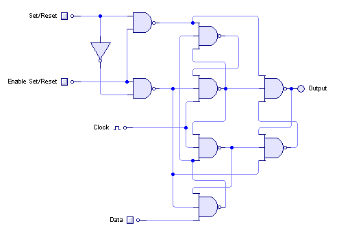
The reason why I got stuck was because I was attempting to build a DTL edge-triggered D flip-flop, and no matter how I tried, I could not build one that contained SET and RESET terminals. I could build one with just a clock and an INPUT terminal, but I could not go any further:
![]()
Enter the Discrete-Component PDP-8
I started researching and building a discrete component CPU/computer when I was diagnosed with schizophrenia in July 2013. The level of detail and concentration you have to come to master prevented me from getting any more delusional. I gave up the project when I started my PhD in 2015. I made another attempt to make a four-phase clock in 2016, but I failed again.
Then when I returned to this project a month ago (Feb 2018), I remembered I came across some schematics for an old discrete-component IBM computer back in 2013, but balked at the idea of using their basic logic element because it used so many bizarre voltages. "It used negative voltages!" I thought. There was no way I was going to be able to manage a project with such whacky logic levels, like negative voltages for positive logic signals. I went down the TTL logic route for five years.
This time, in 2018, I was determined to get further. I knew discrete component computers were built in the 50s and 60s, and I knew they were able to generate clock signals and have multi-phase clocks. All I had to do was find their schematics.
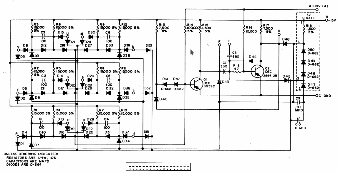
So I did. I found a wealth of resources on the DEC PDP-8. It is a wonderful computer architecture. It has a single accumulator you use with something like 6502 zero-page memory addressing in order to perform calculations. It is very RISC-like with a tiny number of opcodes, and it only contains something like 500-odd gates. So in February I thought it would be a wonderful computer to clone.
...if only I had enough money.
When I found out I could join this TTLers group, I decided I wanted to share my research on the strange DTL architecture of the PDP-8 in the hope it would help somebody.
The Standard Logic Pulse of the PDP-8
Before I start describing the electrical and logical system of the PDP-8, I want to explain how I came to obtain all this information. I retrieved it from pdp8online.org. Virtually the entire library of information required in order to repair, construct or just simply understand the PDP-8, as well as other DEC minicomputers, is all online at that website.
All of the information I have explained here comes from the DEC 1967 Digital Logic Handbook. It is the last digital logic handbook that uses R-series logic. From 1968 onwards, DEC uses M-series logic, which is basically just normal TTL.
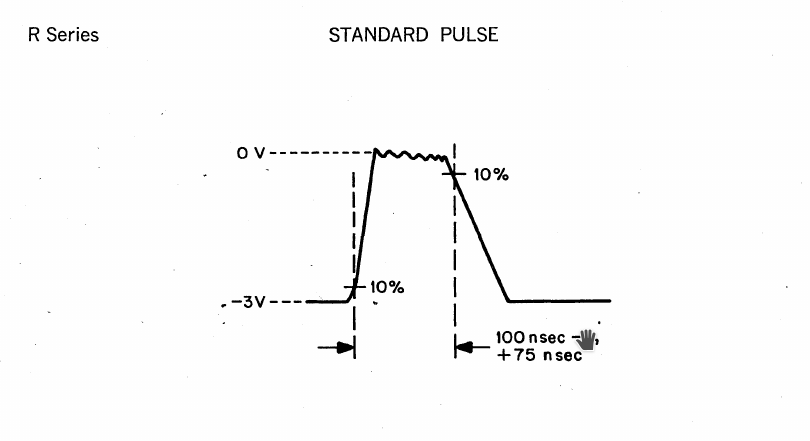
Anyway here is the standard logic pulse of the PDP-8.
![]()
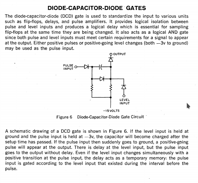
The PDP-8 uses DEC's proprietary R-series logic. As the following diagrams explain, R-series logic takes a -3V signal to be a digital ONE, and a 0V electrical signal to be a digital 0. This is very whacky, and may seem strange, but there's nothing theoretically incorrect about using negative voltages in one's logic system. Virtually any voltage differential can map onto whatever number system you want your computer to use. By the time we get to Diode-Capacitor-Diode gates, the reasoning for -3V = 1 will become apparent.
![]()
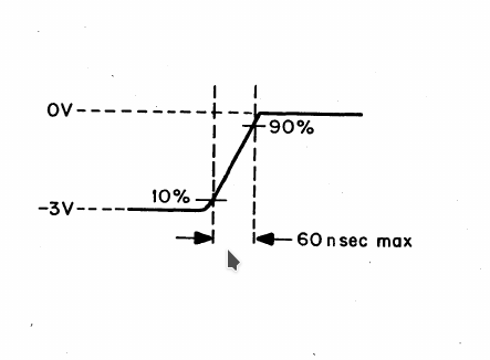
This diagram explains the standard rise and fall time requirements of standard logic pulses in R-series logic:
![]()
The Standard DEC Logic Gate Symbols
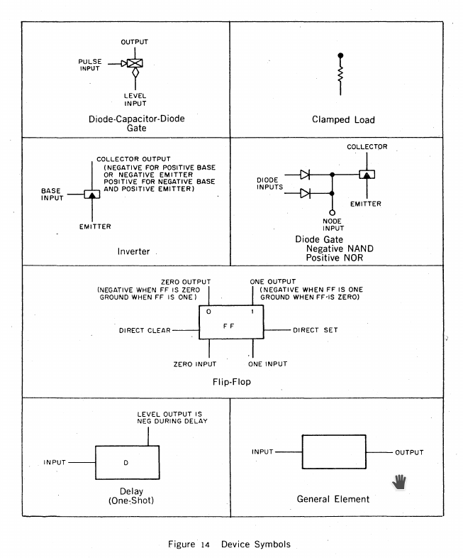
So that the later diagrams and schematics make sense, it is important to understand the symbols for different logic elements that DEC employed in order to describe the R-series logic system. Here is the explanation:
![]()
Here, in Figure 14, we can see (from left to right, down the page) the symbols for Diode-Capacitor-Diode gates (DCD gates), for a PNP transistor, for NAND and NOR gates, for RS flip-flops, for monostable multivibrators, and for general logic functions.
R-Series Logic Signal Symbols
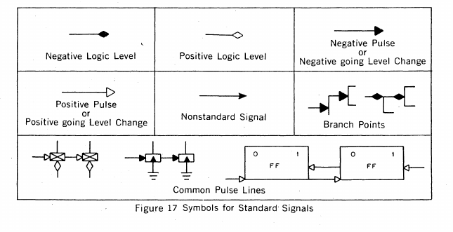
The R-Series logic construction of the PDP-8 doesn't just use standard -3V signals for digital ONEs. It also uses positive logic PULSES, in addition to LEVEL logic signals (in order to edge-trigger flip-flops), and it uses negative PULSES, as well as non-standard signals where it isn't possible to efficiently construct logical elements electrically using standard signals and pulses.
Please find the standard DEC R-series logic signal symbols below.
![]() You can see why I originally dismissed this system in 2013, because it can seem theoretically unparsimonious. It is very promiscuous with its conceptual implementation, BUT, as I now understand, this is for the purpose of making R-series logic computers very easy to construct by hand. This allows the PDP-8 to be constructed with the minimal number of electronic components, and it simplifies the overall electrical schematics.
You can see why I originally dismissed this system in 2013, because it can seem theoretically unparsimonious. It is very promiscuous with its conceptual implementation, BUT, as I now understand, this is for the purpose of making R-series logic computers very easy to construct by hand. This allows the PDP-8 to be constructed with the minimal number of electronic components, and it simplifies the overall electrical schematics.
As you can see, the DCD gates in the bottom part of the diagram are receiving positive logic level signals, and are triggered by positive pulses, and inverters are shown to be receiving negative pulses, or negative-going logical level changes.The R-Series Logic NOT-gate
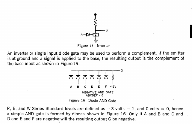
This is the standard inverter of R-series logic. Virtually every other passive logic element is constructed out of this gate:
![]()
It uses a PNP transistor, the exact electrical component equivalents I have found, and it uses far more diodes than in other DTL electronics. In fact, you'll find, when looking at the schematics of the R series flip chips, which I can provide, most of the logic is actually carried out by diodes, with signal voltages to be amplified later by transistors. Very few transistors indeed are used in R-series logic. This may actually be an advantage to the system.
![]()
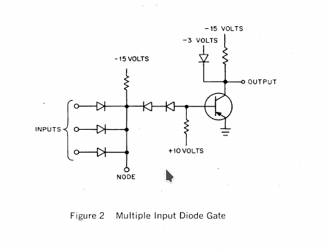
Figure 2 above shows what a multiple input diode gate looks like in R-series logic. With negative signals, this gate operates as a NAND, and with positive signals, it acts as a NOR.
Edge-Triggering: Enter the Diode-Capacitor-Diode Gate
![]()
The diagram above explains the operation of the DCD gate in a sufficient level of detail. Pulses with shorter levels than normal logical pulses trigger the DCD gate, and using DCD gates allow one to be able to sample flip-flops while they are about to be changed. ADDING capacitance to a logical circuit seems like a crazy thing to do, but that is what DEC did.
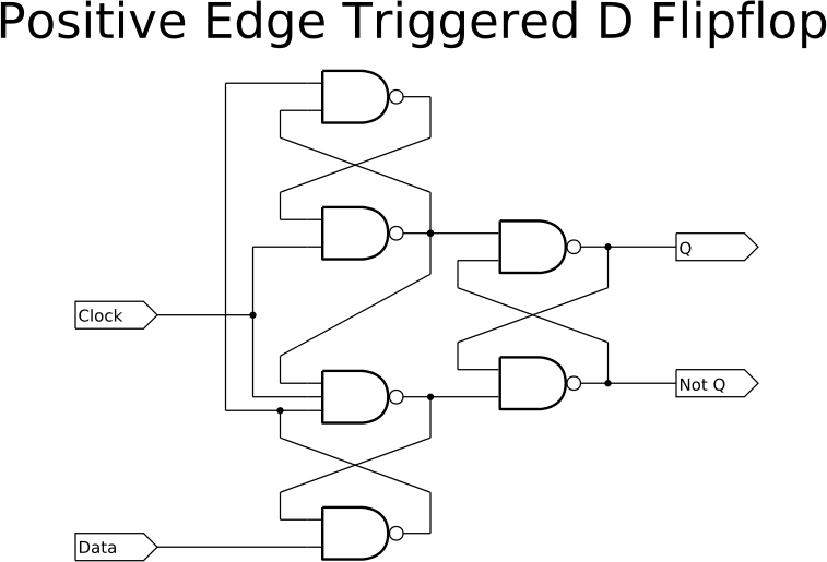
DCD gates are a fairly clever solution to isolating logical inputs and outputs, as well as allowing edge-triggering. Edge-triggering using whole NAND or NOR gates can lead to many many semiconductor components being involved. Remember, using whole NAND gates transforms an logical-level D flip-flop from this:
![]()
to an edge-triggered d flip-flop, this:
![]()
Not only do we now have one more gate, but we also have gates with multiple inputs, requiring more diodes. Nevermind that we haven't dealt with settable and resettable edge-triggered D flip-flops.
![]()
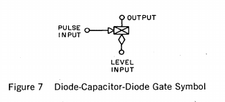
This is the symbol for a DCD gate. As you can see, they operate with POSITIVE logic pulses, and POSITIVE logic level inputs.
Flip-Flops
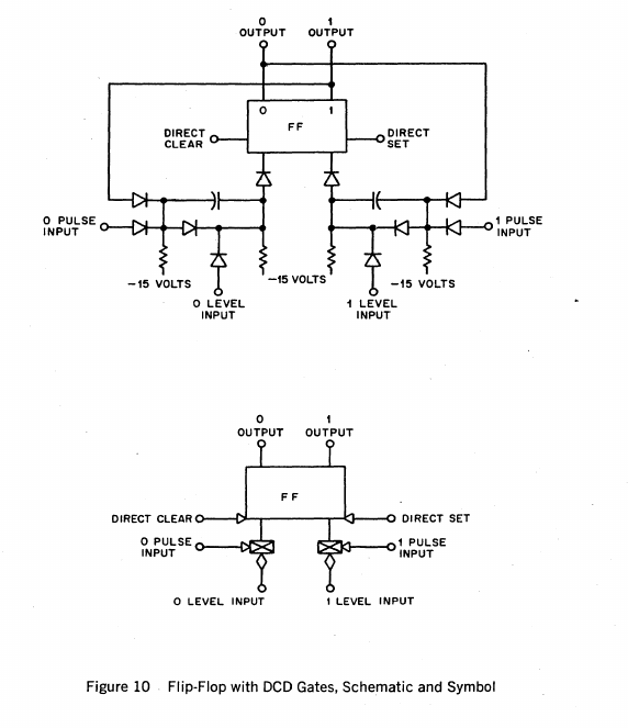
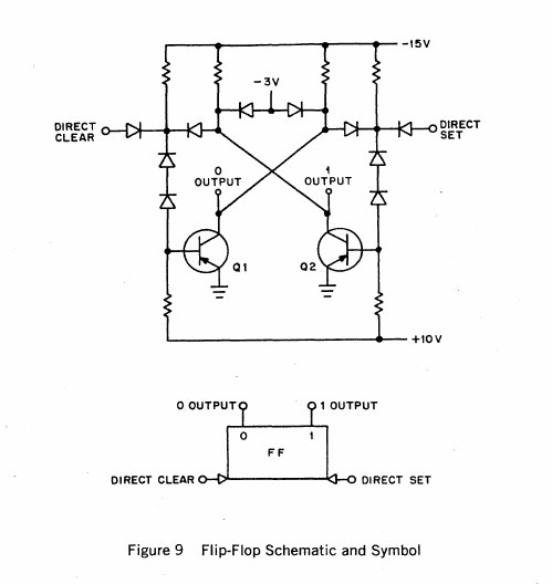
In much the same way as DCD gates allow input-output isolation, and edge triggering with few electronic components, DEC standard RS flip-flops are also very simple in their electrical construction. They use few components, and would therefore reduce the overall size of the PDP-8, as well as its operating power, and heat footprint. The R-series logic RS flip-flop below reminds one of a simple RTL flip-flop.
You can also see the logical symbol for the standard R-series logic flip-flop below.
![]() RS flip-flops are almost always combined with DCD gates, which allow the logic element to perform in dynamic operation. Outputs may be sampled as inputs are waiting to be transferred into the logic element, so DCD gates allow logical isolation.
RS flip-flops are almost always combined with DCD gates, which allow the logic element to perform in dynamic operation. Outputs may be sampled as inputs are waiting to be transferred into the logic element, so DCD gates allow logical isolation. ![]()
As you can see, flip-flops require POSITIVE logic level singals, and POSITIVE logic pulses.
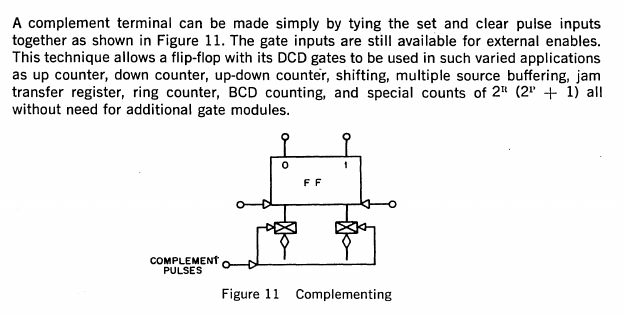
Complementing Flip-Flops
![]()
The power of the DCD gate is apparent here - without any extra components, a normal RS flip-flop can be turned into a complementing JK flip-flop.
Complex Logical Elements
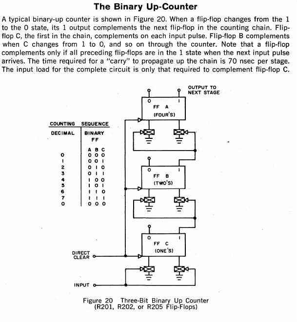
This is a very quick example of how R-series logic flip-flops would be combined into a complex logical element. There are a great many examples in the R-series logic handbook, like settable and resettable counters, etc.
![]()
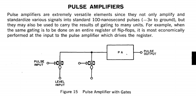
The Legacy of RTL in R-series Logic: Pulse Amplifiers
Because most of the logic calculation in R-series logic is performed by diodes, R-series logic requires analogue electronic elements. The fan-out of digital logic elements is limited, so amplifiers are needed to restore electrical signals to their proper voltage and current rating. All of the standard fan-out capabilities of standard R-series logic flip-flops are in the 1967 Digital Logic handbook, if you're looking for more information.
![]()
This is an example of a flip-chip module which is a pulse amplifier, the R601 module:
![]()
As you can probably gather, it is just 6 DCD gates combined with a transistor amplifier.
Component Substitution
When you look at the R-series flip-chip modules, you're probably going to end up despairing because many of the components used in the modules are now obsolete. I have done my best to scour digikey and mouser to find as close electrical equivalent components for all the major elements of the flip chip modules.
That said, if this does present itself to some people as an attractive electronic logic system, we may just reconstruct all the basic logic elements using easily accessible components.
Webpage with original DEC substitution recommendations HERE: (http://so-much-stuff.com/pdp8/repair/subst.php)
Original DEC Component DEC-Specified Component Substitution My Suggested Substitution D-662 Diode (High Forward Voltage Drop) 1N645 1N4004 D-664 Diode (Low Forward Voltage Drop) 1N3606 SB140 Schottky Diode DEC-3639 PNP Transistor 2N3639 2N4403 DEC-3009 NPN Transistor 2N3009 BC559/BC549 DC-2894 PNP Transistor NONE (!!) 2N4403 (?) Conclusion
If you found any of this useful, please check out my blog at https://bootlicker.party/
-
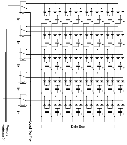
Dynamic RAM with single MOSFET per bit ?
08/20/2016 at 22:54 • 29 commentsRAM is one big problem for "discrete projects". It must be fast, large and cost-effective. There are many types of discrete RAM but none that is based on discrete MOSFET (yet).
Integrated DRAM uses MOSFETs but they differ from the discrete form because of the intrinsic diode with the substrate : it takes two discrete MOSFET to make one normal MOSFET. This would not be cost-effective to use discrete MOSFET to implement classic DRAM circuits.
I found inspiration with the diode-capacitor cell described for the TIM computers :
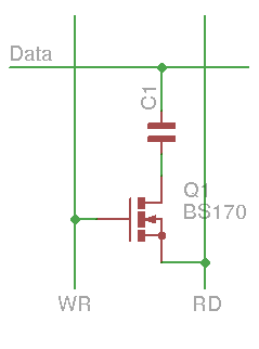
![Diode-capacitor dynamic memory]()
I can't figure out what capacitance was used in the relay-based TIM8. However, with a MOSET-based circuit, the capacitance can be greatly reduced (to 100nF for example) because the required trigger energy is considerably lower. I even have a reel of dual Schottky diodes in SOT23. But I'm not sure about the leakage...
Now, a good MOSFET has a pretty low leakage. I have played around (on paper) and have come up with a topology that replaces the diode with a MOSFET. The gate capacitance is not used but the parasitic diode is !
![]()
Each access cycle takes 2 steps:
- Read and empty the storage capacitor: drive RD high => This pushes the capacitor's lower electrode high, which is then read on the Data line. Probably a threshold current is required to read a "1".
- Write the value: drive the desired level on the Data line, drive RD to 0V and WR to 1 (let the current flow to RD so the lower electrode is 0V).
It's funny that the read phase works a bit like a charge pump...
Data, RD and WR are totem-pole (complementary) drivers. I will have to try different circuits for the sense. The line and column select (demultiplexers) will need a lot of transistors too... But at least it's more compact than the only other MOSFET RAM that I know :-)
Now I wonder what should be the refresh frequency...
Any comment/remark/historical perspective ?
Hackaday TTLers
Where DIY DIP/SSI/MSI CPU makers meet and discuss other TLA (three letters acronyms)


 You can see why I originally dismissed this system in 2013, because it can seem theoretically unparsimonious. It is very promiscuous with its conceptual implementation, BUT, as I now understand, this is for the purpose of making R-series logic computers very easy to construct by hand. This allows the PDP-8 to be constructed with the minimal number of electronic components, and it simplifies the overall electrical schematics.
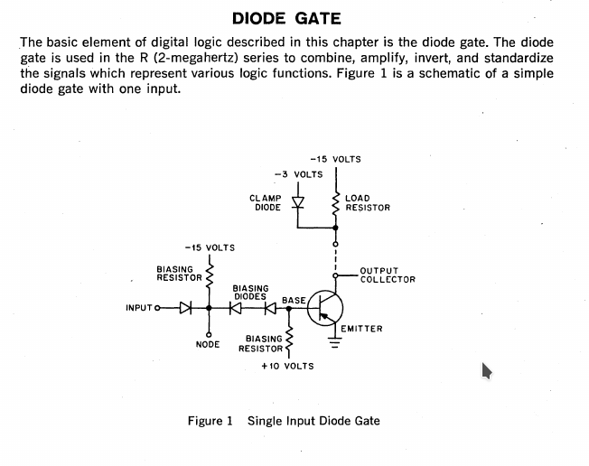

 RS flip-flops are almost always combined with DCD gates, which allow the logic element to perform in dynamic operation. Outputs may be sampled as inputs are waiting to be transferred into the logic element, so DCD gates allow logical isolation.