Operation
On the videos below you can see the currently implemented effects:
On the video below you can see how XMAStar behaves when the button is pressed:
On the video below you can see how XMAStar behaves on under-voltage:
My goals with this project
I wanted to learn the usage of Altium's Circuitmaker. Looking back it was a great choice. After the initial learning period Circuitmakeris a quite powerful free tool for PCB design.
I wanted to build a circuit that is powered with a DC-DC converter using 1 or 2 AA or AAA battery.
For a time I had this little project in mind so I wanted to realize it in this year.
When I was in my early teen years I build a similar star for Christmas. It was a great project. It used discrete transistors to switch the LED's, the transistors were controlled by an up-counter, running from an RC oscillator. It is great to see how technology and my knowledge advanced during the years so now I can design such a circuit with a DC-DC converter, micro controller and current generator based LED driver.
Objectives
- run the circuit from AA batteries
- have at least 1 day of continuous operating time
- use a DC-DC converter
- control the LED's with current generator based LED driver
HW block diagram
On the picture below You can see the HW block diagram.
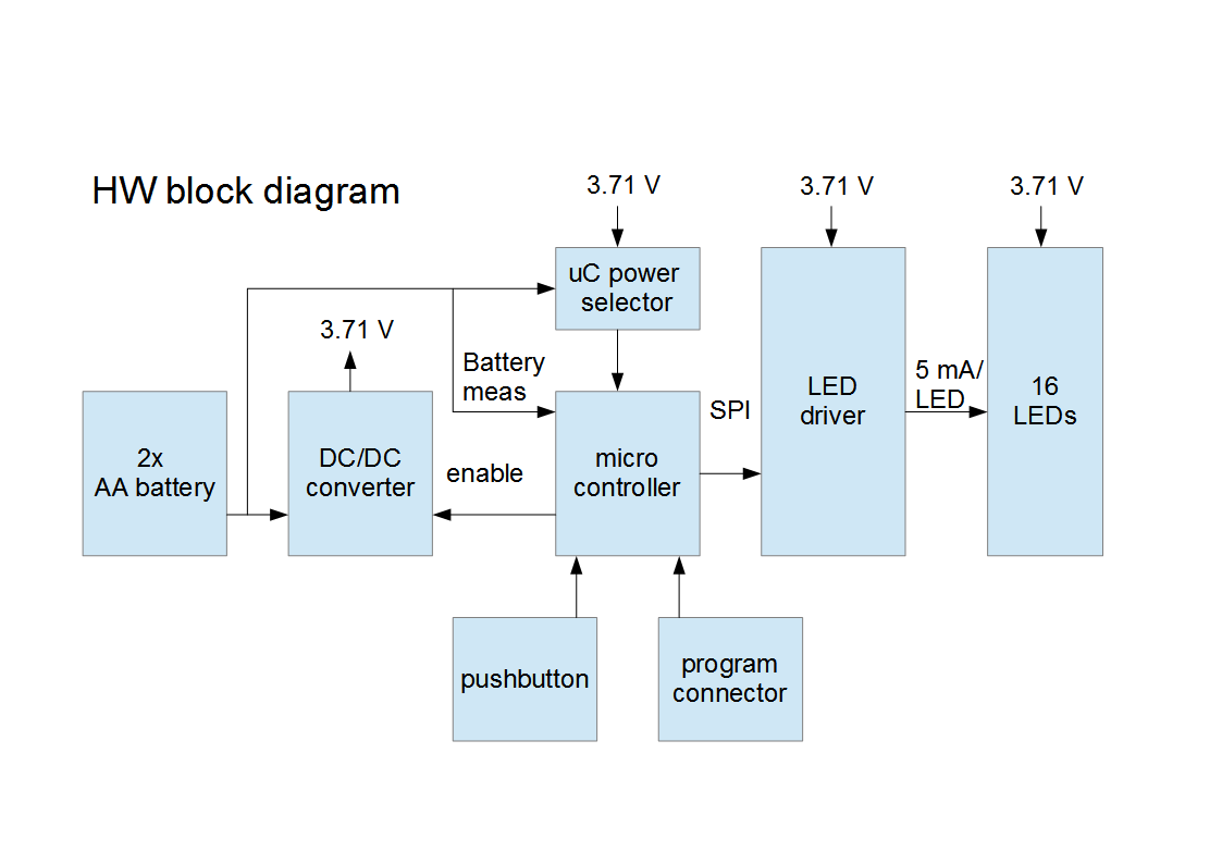
16 LED's are organized in star shape. The circuitry is switching on-off these LED's in various order to create fun visual effects. The color of the LED's are blue, red, yellow and green. I choose through hole LED's because the bulb size of through hole LED's are generally bigger than the SMD ones.
A LED driver IC is used to switch on-off the LED's on SPI commands, and to set the operating current of the LED's to 5mA.
The XMAStar is powered from two AA size battery (Alkaline, NiMH or NiCd). The AA size batteries are chosen because they have a relatively small size, has sufficient capacity to run the circuitry continually for at least 1 day (see the calculation later). Also good AA size PCB solder-able battery holders are available.
The voltage of the two batteries are not sufficient and stable enough to power the LED's therefore a DC-DC converter is used. It converters the battery voltage to fix 3.71V.
Note 1: 3.71V is chosen because the forward opening voltage of the blue LED's can be above 3V, the LED driver needs a minimum 0.6V to operate therefore voltage is chosen above 3V+0.6V
In sleep mode the DC-DC converter is disabled to save power. In disabled mode the DC-DC converter disconnects its output from the battery, therefore the LED driver and the LED's are not supplied, the DC-DC converter consumes around 1uA in sleep mode.
There is power supply selector for the micro controller. In sleep mode when the DC-DC converter is disabled the micro controller is running directly from the battery. If the DC-DC converter is enabled the micro is running from the DC-DC converter output. The power supply selector is implemented with two Schottky diode.
There is micro controller which has three main functionality
- it sends SPI commands to the LED driver to switch on-off the LED's in various orders
- it handles a push button.
- it checks the voltage of the batteries, if the battery voltage drops below a certain level than the micro switches off the DC-DC converter and enters sleep mode
Since in sleep mode the micro runs directly from the battery a low power type PIC is used: PIC16LF1703 which can operate down to 1.8V.
Note 2: the upper voltage limit of this type of micro controller is 3.6V, subtracting the voltage drop on the power supply selector Schottky diode from the 3.71V supply voltage we are just below this limit.
There is one push button connected to the micro. By pushing this button the speed of the LED switching can be adjusted and the circuitry can be put in sleep mode. Meaning of push button presses respectively :
“Low speed state” → “Medium speed state” → High speed state” → “Sleep state“ →“Low speed state”
Programming connector: a usual, dedicated ICSP programming interface is used to be able to debug and program the micro.
Schematic
On the picture below you can see the schematic of XMAStar:
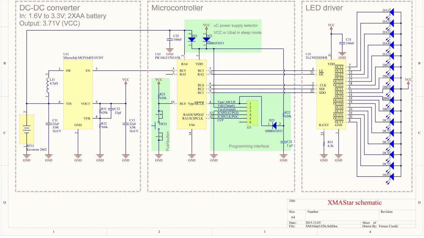
I tried to isolate the main blocks therefore I added a grey dashed line frame around them to easily identify which block is doing what.
I used Altium's Circuitmaker for creating the schematic.
I have tried to reuse the same component values when it was possible.
I have added the 100nF capacitors (C_22 and C_31) after the PCB design freeze, so they are not on the PCB, I just solder them on the IC pins directly.
Software static architecture
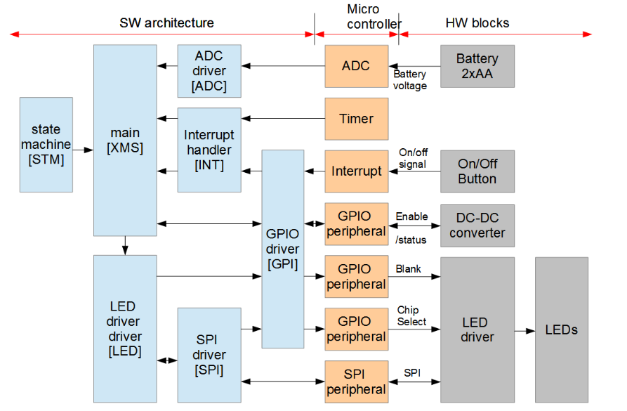
On the picture below You can see the software static architecture: the software units building up the SW system and the main connection between them. I have also displayed the HW-SW interface too: which micro controller peripherals are used and which HW component it connects to.
Each SW unit has a 3 letter unique identifier. Below the picture You can check what is the functionality of these SW units.
ADC:
- inits the ADC peripheral
- provides ADC conversion result for the upper level modules
- the ADC converted value of the analog voltage of the following sources are provided:
- PIN connected to battery voltage measurement
- internal voltage reference
GPI:
- initialize the registers corresponding to GPIO PIN handling
- provides interface for getting the logical level on the PIN connected to the push-button
- provides interface for setting PIN's to logical low or high level of these signals:
- DC-DC converter enable
- SPI Chip Select signal
- LED driver enable
SPI:
- initialize the SPI peripheral according to the protocol needed for the LED driver
- provides interface for sending data to the LED driver
- receives data from the LED driver
LED:
- currently this driver is not used, it planned to be the logical abstraction layer for the LED driver it could handle the“LED open detection” and “over temperature warning” signals of the LED driver
INT:
- initialize a timer to provide a periodic interrupt for „tasking”
- initialize the interrupt on pin change function of the micro to be able to handle the button press interrupt
- handles button press interrupt
XMS:
- this is the main SW component where the main() function is located
- it contains the config register settings
- it inits the PIC clock to 250 kHz
- it calls the init function of the other SW components
- on the periodic timer interrupt it performs the operations and function calls needed in the various main state machine states
STM:
- this driver contains the various LED blinking patterns in the form of 16bit arrays
- upon a function call it provides the next pattern on its interface
- it also updates the main state machine state on a button press or a function call
Software dynamic behavior: main state machine
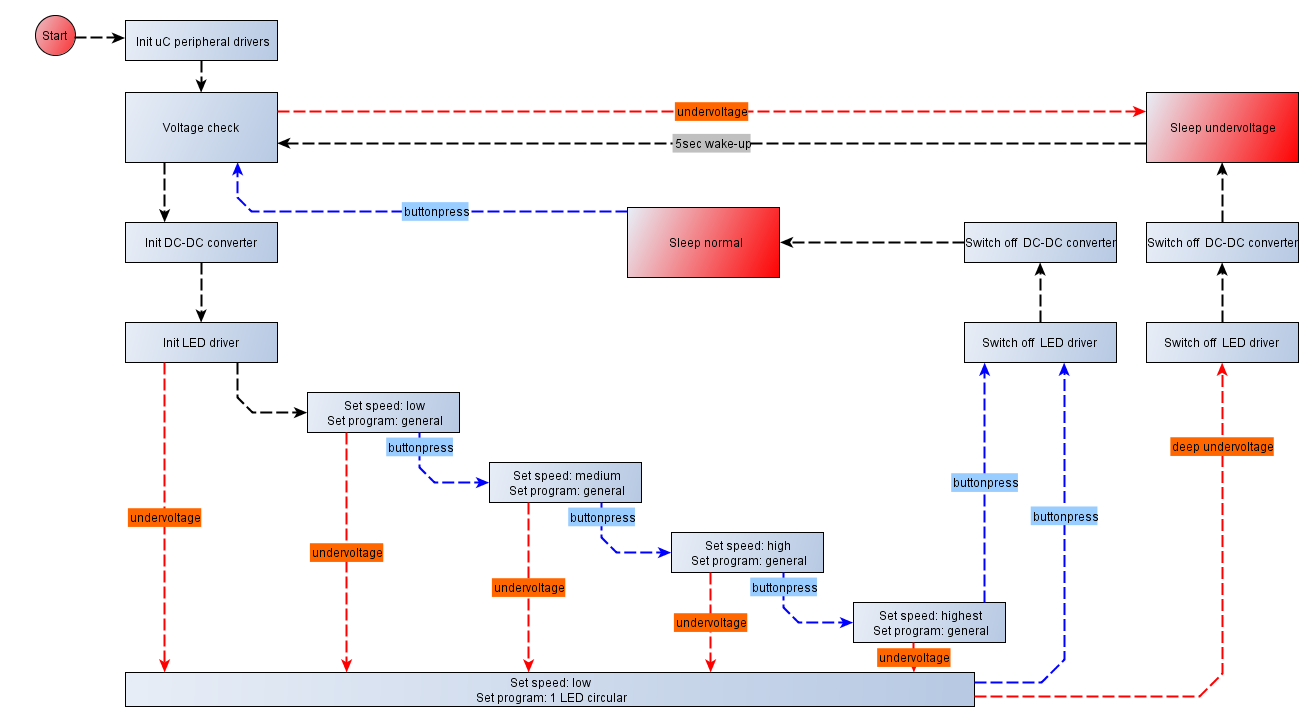
On the picture below the main state machine can be seen.
State changes happen
- automatically (black lines)
- when a button is pressed(blue line)
- or when there is under voltage (red line)
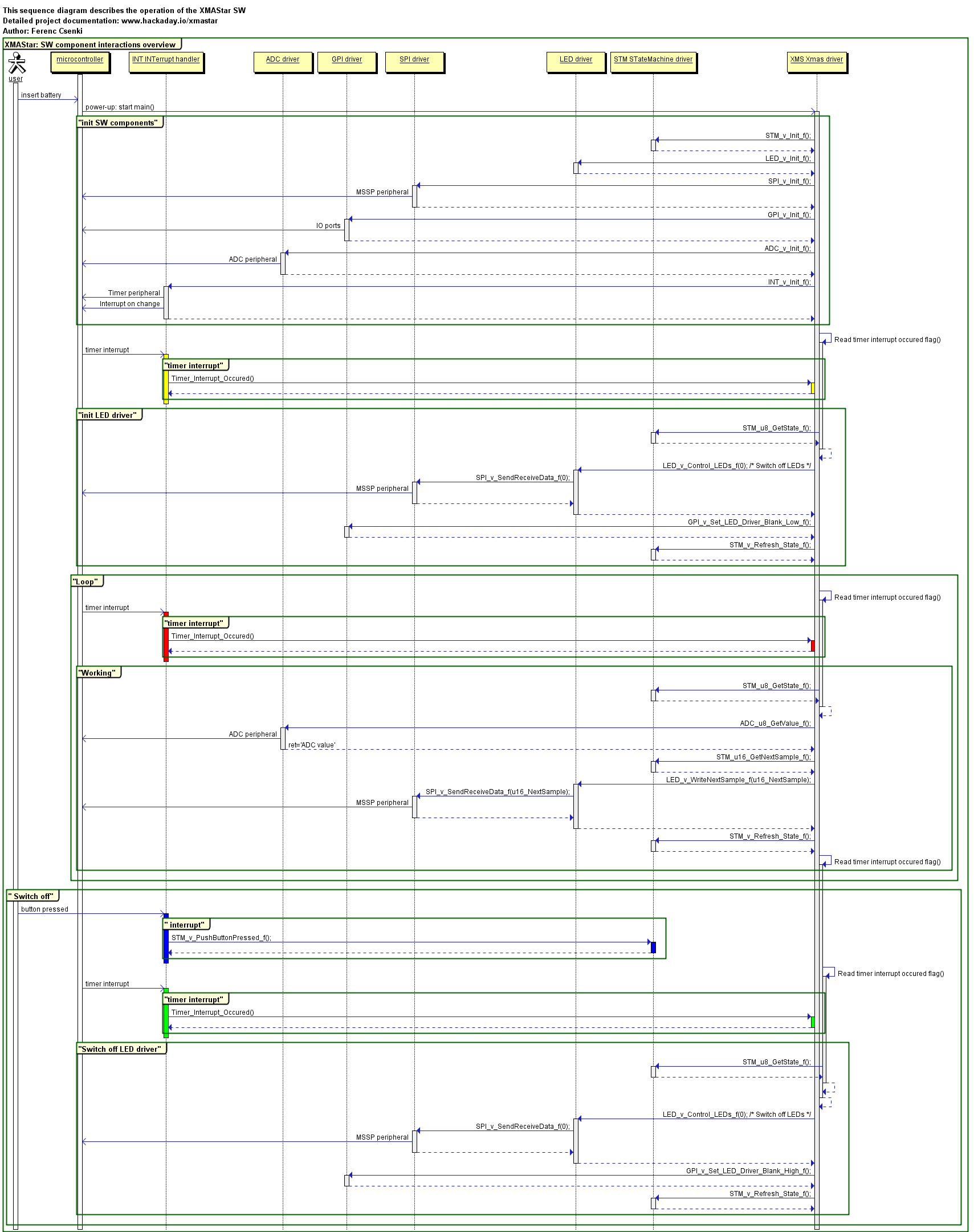
Software dynamic behavior: sequence diagram
On the sequence diagram below, you can see what happens between the SW components after start-up during normal operation and switch-off.This is the first version of the sequence diagram I created before coding. I did not updated it further when I started coding but changed a few minor things in the code.
System design: controlling the LED's
There are 16 LED's on the PCB.
The designator numbers of the LED's can be seen on the picture below:
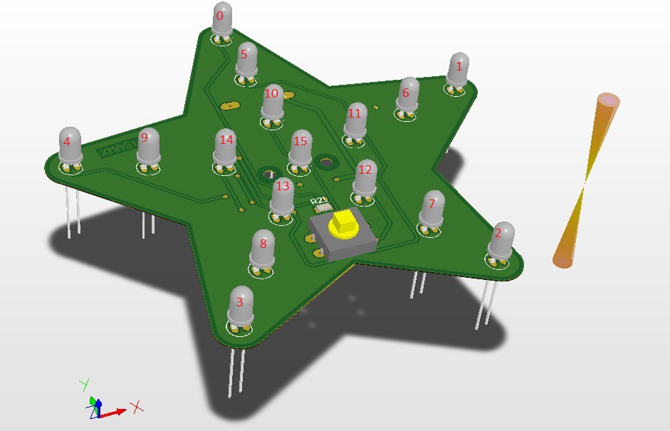
The LED driver is controlled with a 16bit wide SPI message, in this message each bit corresponds to one LED. When the bit is 1 the corresponding LED is switched on when the bit is 0 the LED is switched off.
| bit | 15 | 14 | 13 | 12 | 11 | 10 | 9 | 8 | 7 | 6 | 5 | 4 | 3 | 2 | 1 | 0 |
| LED | 15 | 14 | 13 | 12 | 11 | 10 | 9 | 8 | 7 | 6 | 5 | 4 | 3 | 2 | 1 | 0 |
To create a sequence we send out these messages to the LED driver with a given speed.
The base speed is 62ms. The speed can be adjusted between 81ms and 255*81ms.
For example the program which is circularly switching on one LED at a time looks like the following:
0b0000000000000000
0b0000000000000001
0b0000000000000010
0b0000000000000100
0b0000000000001000
0b0000000000010000
0b0000000000100000
0b0000000001000000
0b0000000010000000
0b0000000100000000
0b0000001000000000
0b0000010000000000
0b0000100000000000
0b0001000000000000
0b0010000000000000
0b0100000000000000
0b1000000000000000
END

Speed: 2*81ms
System design: rough operation time calculation
| Input voltage (battery voltage of 2 AA cells): | 2.6 V |
| Output voltage: | 3.71 V |
| LED operation current: | 5 mA |
| Average number of LED's switched on: | 8 |
| Sum currents of LED's: | 8 * 5 mA = 40 mA |
| LED driver's current consumption: | 8 mA |
| PIC current consumption: | 1 mA |
| Sum current consumption: | 1 mA + 8 mA + 40 mA = 49 mA |
| DC-DC converter efficiency: | 85 % |
Note1: The picture below is from the datasheet of MCP1640:
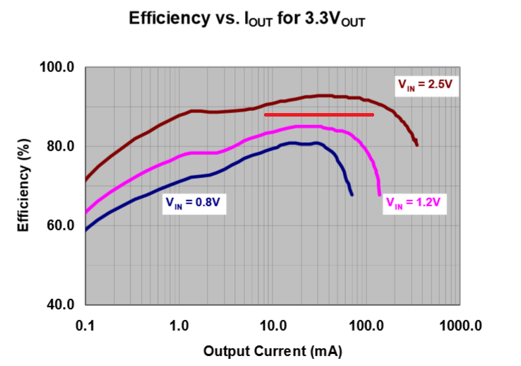
We operate around the red line, so the DC-DC converter efficiency is taken as 85 % in the calculation.
| Seconder power: | 49 mA * 3.71 V = 182 mW |
| Primary power: | 182 mW * 0.85 =214 mW |
| Primary current (battery current): | 214mW / 2.6 V= 82 mA |
| Battery capacity: | 2000 mAh |
| Estimated operation time: | 2000 mAh/ 82 mA= 24 hours |
On component selection
During prototyping I came to the conclusion that the smallest pitch distance (contact switch) size I can easily hand solder is around 0.5mm.
So I have to change the LED driver and DC-DC converter type during prototyping because initially I choose smaller packages that were impossible to correctly solder by hand.
System design: voltage level handling in ADC driver
Two things happen when the battery voltage starts to drop:
- at 2.176V (1.088V per cell) we enter low battery mode, this means that we circularly switch on only one LED at a time indicating that the battery is depleting
- at 1.920V (0.96V per cell) we completely switch off the DC-DC converter
When the battery voltage start to increase:
- at 2.176V we switch back the DC-DC converter again and start normal operation
Note1: there is a 2.176V-1.920V = 0.256V differences between the DC-DC converter switch on-off levels. This serves as a hysteresis. When we have a noisy battery voltage measurement no unintentional switch on-offs happen.
Note2: the rising of the battery voltage is not a normal case when using AA cells, this function is just added for test purposes: when the circuitry is operated from an external adjustable power supply
There are two constraints implementing this functionality:
- the PIC do not have a division instruction
- there is only one reference voltage in the system, the PIC's internal 1.024V reference voltage
So I use the following algorithm:
Battery voltage on AN3 pin is ADC converted:
battery_ADC = U_battery/U_ADCref*2^12
Battery voltage on internal (1.024V) voltage reference is ADC converted:
1V024_ADC = U_voltref/U_ADCref*2^12
0.128V is calculated:
1V024_ADC shifted right by 3 (1.024V/2^3=0.128V):
0V128_ADC = 1V024_ADC >>3
0.256V is calculated:
1V024_ADC shifted right by 2 (1.024V/2^2=0.256V):
0V256_ADC = 1V024_ADC >>2
2.048V is calculated:
1V024_ADC shifted left by 1 (1.024V*2^1=2.048V)
2V048_ADC = 1V024_ADC <<1
1.920V is calculated:
1V920V_ADC = 2V048_ADC - 0V128_ADC
2.176V is calculated:
2.176V_ADC = 1V920V_ADC + 0V256_ADC
Note: the algorithm above is independent from the actual U_ADCRef voltage which is the Vcc voltage in our case.
PCB design
The special PCB shape, the two sided construction and the manufacturing constraints (clearance, minimal trace width, etc) put a restriction on the PCB design. So I could not really optimize for better grounding, recommended layout, etc.
I was using Altium's Circuitmaker for schematic and PCB design. One neat feature of Circuitmaker I want to highlight is the automatic PIN swapping feature which helped a lot. PIN's with similar functionality (e.g the outputs of the LED driver, GPIO PIN's) can be grouped together. Within the group the PIN's can be swapped automatically for better suite the PCB layout (trace length within the group can be minimized). Of course the PIN swapping has to be considered in the SW afterwards.
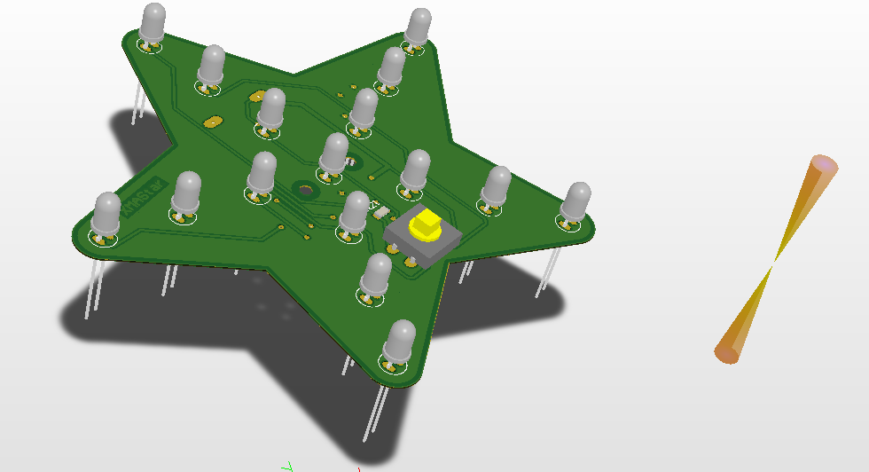
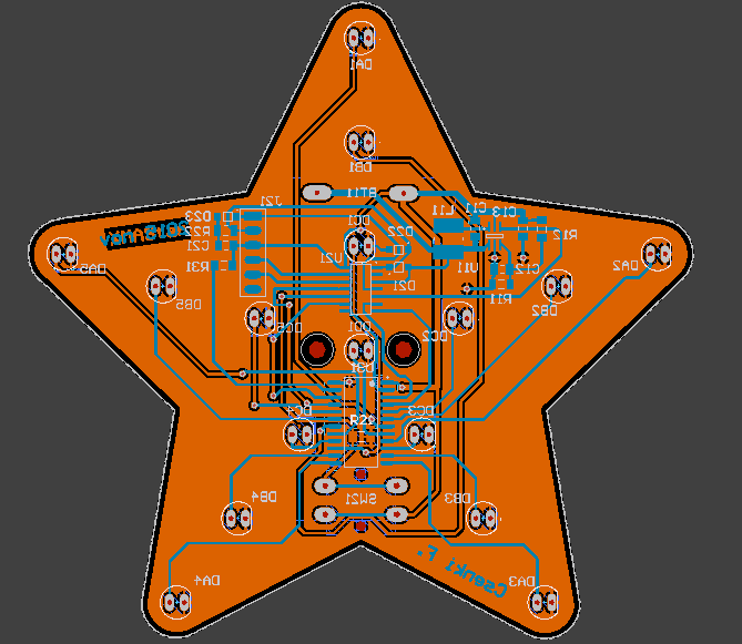
You can find the schematic and PCB under Circuitmaker community vault for free.
Search for the following tag: 'XMAStarLEDs', under Start/ Popular, new and watched projects 'show more'/ Community/ Projects.
Scope pictures
DC-DC converter signals
| Yellow signal | Battery | Battery voltage |
| Blue signal | Vdd | Micro controller power supply |
| Red signal | Vcc | LED driver power supply |
| Green signal | Enable | DC-DC converter enable signal |
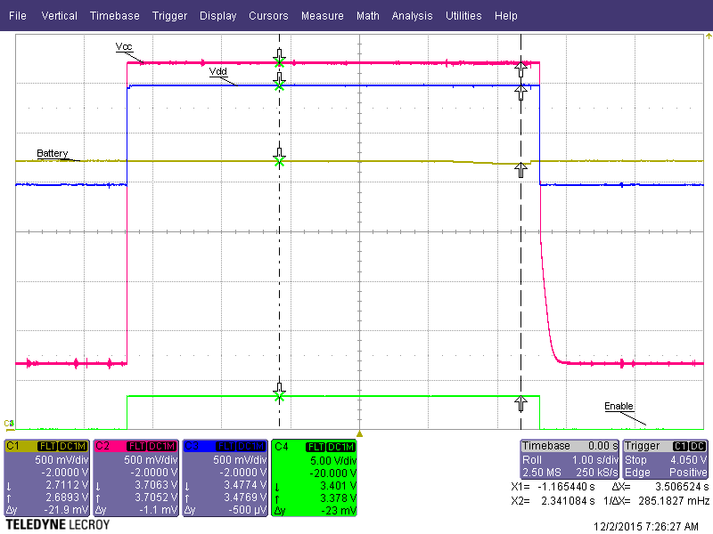
On this measurement it can be seen that the battery is ~2.7V.
At around 1.5sec the DC-DC converter is enabled: the green line goes to high level. The DC-DC converter output (Vcc) gets 3.71V.
The blue line is the output of the micro controller power supply selector.
It can be seen that the blue line is one diode drop smaller than the battery voltage or Vcc (whichever is higher).
LED driver signals
| Yellow signal | LED1 | LED driver output 1 |
| Blue signal | R_ext | R_ext pin of the LED driver (reference current setting PIN) |
| Red signal | Vcc | LED driver power supply |
| Green signal | LED2 | LED driver output 2 |
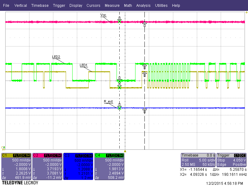
On this measurement it can be seen that the Vcc is ~3.71V.
The R_ext pin of the LED driver is 1.21V.
This voltage is the reference which sets the ~5mA current of the LED's.
The LED1 and LED2 signals are two outputs of the LED driver, when these signals goes lower (~1.9 and ~1.8V) than the 5mA current of the LED's are reached: the LED's are switched on.
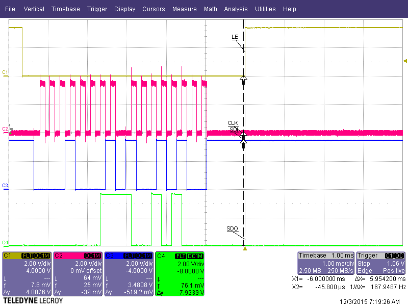
SPI signals
| Yellow signal | LE | latch enable signal |
| Blue signal | SDI | serial data input |
| Red signal | CLK | clock signal |
| Green signal | SDO | serial data output |
Run-time
| Yellow signal | Tasking | this PIN is set to high when functions are called |
| Blue signal | SDI | serial data input |
| Red signal | CLK | clock signal |
| Green signal | SDO | serial data output |
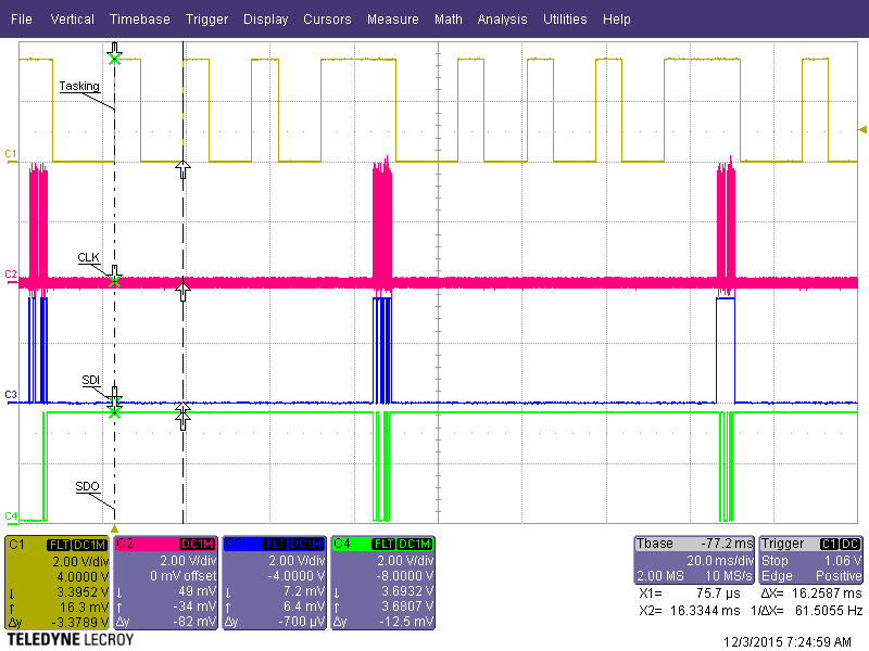
On this measurement the tasking can be seen. There is a periodic ~16.2msec timer interrupt. After this interrupt the functions needed for the operation are called. At the beginning of these function calls a PIN is set to high. When the functions are executed the PIN is set to low. This PIN is with yellow signal on this measurement.
The SPI signals are also on the measurement. We are in the fastest LED blinking operation state of XMAStar. It can be seen that an SPI messages is intended to sent at each 4th interrupt.
It also can be seen that the execution time of the functions are takes more than 16.2msec when an SPI message is sent, resulting in that one interrupt is lost, therefore the SPI message is sent with ~5*16.2ms, around ~81msec. This can be called a timing bug, but I did not correct it since it do not cause noticeable difference in the operation.
Tools used
In this chapter the open-source licenses and permissions as well as any applicable third-party licenses/restrictions are documented.
I used only free tools for creating the design and documentation.
| Documentation, drawings: | Open office 4 |
| Schematic and PCB design: | Altium's Circuitmaker |
| Programming: | C language, C99 |
| Source file editing: | MPLAB X v3.05 |
| Code compilation: | MPLAB X xc8-v1.34 |
| Drawings: | yED 3.11, ArgoUML |
 hkdcsf