Jason Westervelt
-
What a homebrew computer can do... Fractal Art!
07/14/2017 at 05:53 • 0 commentsI was talking with my friends in Slack about writing some interesting code for rhombus since I've been away from the project for so long. This is what came out of 3 hours of coding and a couple cans of Red Bull.
Enjoy! -
Much needed updates...
07/11/2017 at 20:52 • 0 commentsMy sincere apology for the extended delay. Job and life kinda smacked me upside the head at the same time. :/
I decided that the original intent of this project was to make something minimalist, open-source and easily replicated by the masses. To that extent, the current state of rhombus meets those goals, however I need to do some polish on the code as well as the hardware, and do a good deal of documentation explaining how to get ROMs flashed, how to program the CPLD, etc. Ideally I'd love it if someone with minimal experience could stumble across this project when searching for something to do with an old 68020 that they found inside a laser printer or other salvage... and make something that actually works and can serve as a learning aid.
But whilst working on this project, which has been a learning experience for me, I've thought about many things that I'd love to do with the system that I have built. Things like booting linux, which require an MMU, as well as interfacing with a bus such as VME, will take this project out of the realm of minimalism.
The two systems will remain closely related, enough so that starting a new hackaday project would seem unwarranted. One thing that hackaday.io seems to lack is a way of versioning a project. This kinda drives my inner OCD demons nuts. What I plan on doing is splitting the project into rhombus v1 and rhombus v2, with v2 being focused on modularization and adaptation to the VME bus, as well as development of peripherals (SID based stereo sound, SCSI adapter, network adapter, etc). This should let my audience have the best of both worlds... a simple system one can build to experiment with homebrew computing, and a more complex system which can be put to use doing real-world tasks.
All that being said, I have a board which I need to send to Oshpark. It's a full size VME board and has dimensions of about 13.5x9.5 inches. That is a $600 investment to run off a board of this size, even though I get 3 boards in return. This is another reason for the delay in my update. I've been going over this board design multiple times to make certain that it is a perfect as I can get it before sinking the money into a first prototype run. Once the board is received, populated, and tested, I'll post pics as well as documentation. I have built this board to be a generic VME interface with surface mount LEDs on every single VME line, mainly for the geek factor but also because I figure why not... I'm already blowing half a kilodollar on the board. The board will allow me to use different CPU modules, perhaps an x86 or some other architecture, and just reuse my existing VME chassis, backplane, and peripherals. Or, if somebody else wants to take a stab at a homebrew VME board for a particular CPU, they will have a nice looking mainboard to start from.
The goals are thus pretty straight forward. For v1, I need to do code cleanup, documentation, and make the hardware a bit more tidy. For v2, I need to get this board sent off, then get it into my VME chassis and tested. Once that is done, I will start focusing on v2 and take suggestions from the community as to what peripheral to build next. I have great interest in building just about anything related to computers, and I am certain that whatever is suggested will serve as a learning opportunity for myself and others.
Additionally, I have noticed that hackaday.io has added a file attachment space for each project, so I will work on adding resources from my github.com account here locally. -
New board designs underway
01/22/2016 at 21:35 • 12 commentsI've finished the schematic for the two boards and once the parts that I have on order arrive, I will begin making wire-wrapped prototypes prior to sending the boards off to be fabricated. Overall, the design is a lot more flexible and a lot less complicated that I thought it would be.
The VME board itself will be somewhat expensive due to the physical size of the board. For this reason, I want to make the board as flexible as possible to allow for future changes without having to spin off a new board. While rhombus is a 68020 board, I do plan on moving up to a 68040 for my next project, and I'd prefer having a VME interface that will accept the new CPU board with no physical changes. The board itself is rather simple... a CPLD, an EPROM for doing the address modifier lookups, and the bus buffer/transceivers.
With regard to rhombus, the board is actually going to end up being smaller than my current wire-wrapped prototype, mainly due to switching to the PLCC-packaged MC68901 and ROM. RAM is going to be tested with DIP parts, however it will be replaced with 4x 44-TSOP packaged ICs once I run off copies of the board. There will be a need for pull-up resistors as some of the CPLD outputs are needing to be changed to open collector as they will also be potentially driven from the VME bus header.
I also plan on adding a flash configuration rom and creating a basic configuration utility, but i'm currently debating a few design choices. Primarily the flash rom will be useful for storing information about add-in cards on the VME bus, and thus generating the necessary address modifier codes. Additionally, it will store things found in traditional PC BIOS, such as date/time, serial port configuration, etc. As such, there is potential need for the ROM to exist on the stand-alone CPU board as well as on the VME adapter board. I'm thinking of going with the latter, and allowing the CPU board to read data from the flash ROM if it is present and reverting to either jumpered values or values programmed into the CPU-board's EPROM if the flash device is not present. -
VME Documentation Voodoo Deciphered
01/19/2016 at 22:28 • 7 commentsSo, after going through a ridiculous amount of documentation, I had to resort to a handful of schematics for 8-bit port cards which show that D0-D7 on the interface, whether UART or SCSI or network, are connected to D8-D15 on the VME bus. The schematics that I have seen would indeed work with the diagram provided on my prior log entry. At least I have a path forward now.
The next design phase is relatively straight forward. I have two 6U prototyping boards which will be used for wirewrapped versions of my main CPU board as well as a simple FT245 UART interface card. The UART is just to verify that I can get the VME signals all working as expected. Once the UART is verified to work, it will be moved to the main CPU board and the prototyping board will be cleared up for development of newer interface cards.
The CPU board is receiving an overhaul. I am moving to a 16bit data bus for the EPROM, and 32bit data bus for the RAM. In addition to this, the 68901 is being changed to the PLCC part since the DIP package is considerably larger. I am also adding my keyboard interface to the CPU board.
The board will remain minimalist in nature to allow a solid starting point for other tinkerers, but the expansion header on the board will mate with my VME interface board which will contain the bus transceivers as well as the necessary glue logic within another CPLD. The VME interface board will contain much blinkenlights, with the intent of providing visual feedback as to the status of each VME signal.
That said, here are a few shots of the 10-slot VME backplane that I am using. This backplane is passively terminated with 330/470 ohm resistor pairs on each end of each non-daisy-chained line. Between both connectors, there are a total of 96 lines which are terminated. The serial resistance between 5V and GND at each end of each line is 330+470 = 800 ohms. 96 lines * 2 terminations (one at each end) yields 192 parallel resistances of 800 ohms each. Doing that math, that's an effective resistance of 4.167 ohms between +5V and GND. Gonna need over 1 AMP just to drive the backplane. :)
When I first obtained the backplane, I was shocked by just how heavy the thing was. As I looked it over, I started to notice even more interesting traits. The resistor packs are all socketed. I guess this is to be expected as I would have done the same. Aside from the resistor pack sockets and the 2 dozen capacitors, nothing else is soldered. The screw terminals, the jumper headers, the giant 96pin VME bus connects... each are press-fit into through-plated holes. The first photo shows this upon examination. I guess the parts can be pulled and replaced should the need arise. I'm quite happy with this board, especially seeing as I obtained it for $10.![]()
![]()
![]()
-
Time to bust out the books...
01/12/2016 at 03:30 • 29 commentsIn preparation for the next revision of my hardware, I'm looking at making use of a standardized bus. I have a VME chassis and backplane, so I might as well make use of it. There are a few issues that I am running into, but I am certain that I'll get them figured out with a little reading.
Basically what it boils down to is that A0 (address 0 line) is not presented on the VME bus. This leads one to believe that everything is 16bit data width or higher on the bus. There is an issue with that thought, specifically that 8bit cards and peripherals DO exist for VME systems.
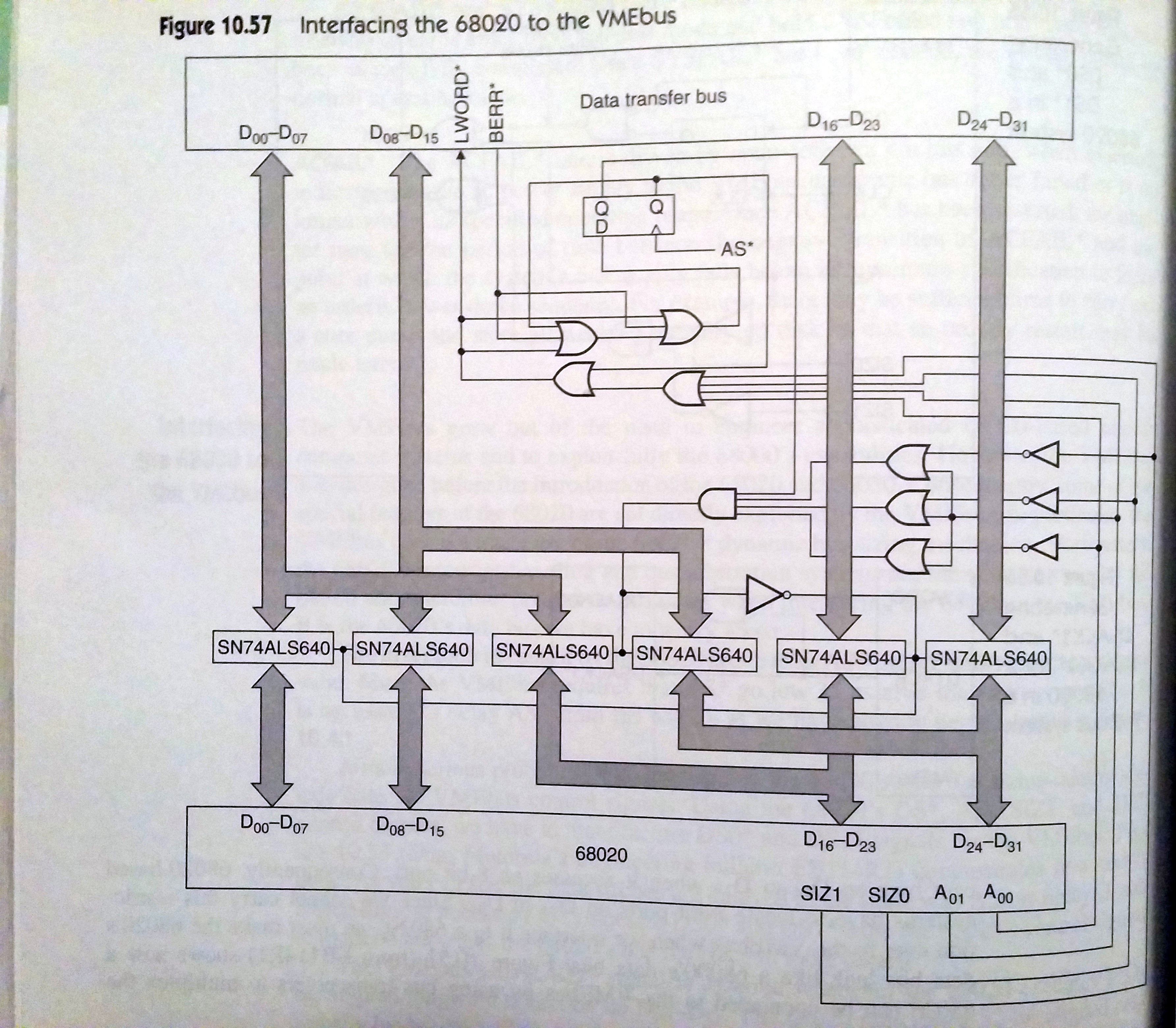
The documentation that I have from Motorola shows that, because the 68020 and higher are capable of 32bit data operations, that a few things have to be addressed when interfacing these CPUs to a VME system. One such difference is that the 8-bit data bus is present on D24-D31... 16-bit on D16-D31. That's fine, a few transceivers and supporting logic should fix the byte presentation to the CPU... and in fact the documentation that I have proposes just that...![]()
The problem is that the documentation shows D0-D7 on the VME bus going to D16-D23 on the CPU and VME D8-D15 going to CPU D24-D31 for a 16 bit operation, but for an 8-bit transfer, VME D0-D7 still end up going to D16-D23... not D24-D31 as I'd expect.
I find it hard to believe that the documentation would be so horribly flawed, but it wouldn't be the first time that I've run across a spectacular booboo in documentation. Perhaps it is possible that 8-bit devices on the VME bus are actually attached to the upper byte, and thus D8-D15 on the bus ends up getting placed on D24-D31 on the CPU. -
keyboard controller almost functional
12/29/2015 at 02:55 • 0 commentsI've got a couple of quirks to iron out with my keyboard controller, but it is almost working. I should have it completely operational sometime tonight or tomorrow. I elected to go with that old intel N8042 that I found, and it looks like it is going to be a very useful part for this project.
The rev1 board is being designed at the moment. I elected to go with 3 parts which are in a PLCC44 or PLCC52 package:- The first is the intel N8042 keyboard controller. This has linux support. The good part is that I will work to emulate this part with one of my 5V tolerant PLCC44 Xilinx CPLDs. This will give folks the option of using either part should they elect to build one of these systems once I get the board files online.
- The second is a Hitachi HN27C4096CC-12 UV EPROM which is a 2MBit (256Kx16) PLCC44 part. Obviously this means that I'm extending my ROM data bus to 16 bit. :)
- The third is the PLCC52 packaged version of the MC68901. I really like this part, and since I haven't really found a linux driver for it, I certainly plan on using this board as an excuse to write one.
In addition to these 3 PLCC parts, I'm also throwing in 4x K6X8008C2B-UF55 These are 1Mx8 55nS SRAM, so I will end up with 4MB of SRAM, likely 0 wait-state via a 32bit data bus. Also being thrown into the mix is an FT245 USB FIFO. This definitely has linux support and will be my initial console once I get uClinux up and running.
-
System clock requirement
12/27/2015 at 02:00 • 2 commentsIn preparation for eventually booting uClinux (and full linux once I get my MMU and dynamic ram controller built), I'll need a system clock of sorts. I'm not too terribly familiar with how linux deals with the system clock/timer, but I am guessing that an interrupt would need to be triggered every so often... 1khz? 100hz? Anyone know the juicy details on what is needed from both a hardware and a configuration aspect?
-
It's always the little things...
12/26/2015 at 05:04 • 0 commentsI managed to fix the input issue...
The device table includes the device name, such as "CON_IN" and "CON_OUT" for console input/output. When matching was being performed, I foolishly was matching on 8 characters and padding shorter names with spaces. I inadvertently placed a single space after each name, giving "CON_IN " a length of 7 which was causing it to fail during the device lookup. Ooops. I'll be moving these to null-terminated strings in the future.
Things will pick up in pace a bit once I get the functionality from the old monitor into the rewrite. I'll keep the old monitor around since it is pretty simple and easy for a "novice" to understand. The whole purpose of this project is to trailblaze so newcomers can have a shot at doing something which may seem quite intimidating at first. -
Alternate monitor in the works...
12/25/2015 at 11:52 • 0 commentsI have been working on a rewrite of the monitor. There were a couple of deficiencies which would have impeded development later on.
The new monitor uses generic I/O functions for devices, and builds a device definition table in RAM which contains the device's address as well as pointers to the I/O handling routines for each device. The system input and output devices can thus be changed easily while the system is up and running... useful if the user wishes to load s-record data over a separate device for instance.
To my amazement, the output function worked just fine after this massive rewrite. Something is wrong in the input, however, as the 'getline' function is ending prior to receiving any input from the serial port, throwing the thing into a massive loop as it sends a prompt over and over again. Too exhausted to continue debugging it tonight. It's probably some stupid little oversight... -
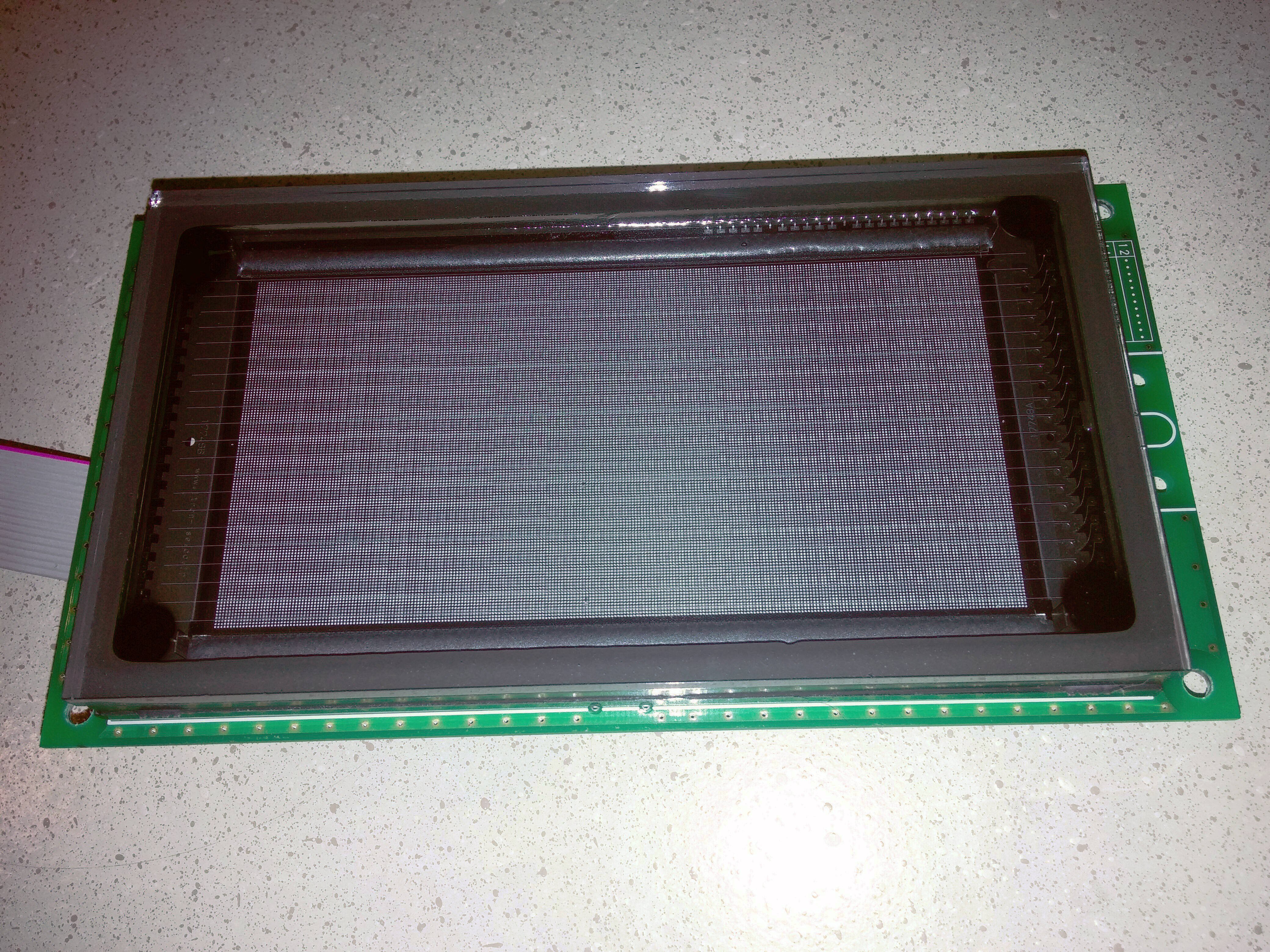
Nothing says energy inefficiently quite like...
12/25/2015 at 05:06 • 4 comments...a big beefy vacuum fluorescent display!
![]()
While this is going to be attached to my board, it really isn't part of the core project. I'm re-writing my monitor to allow for a generic I/O method which will allow the user to toggle between input and output devices. The user can use a serial port for input and output, or switch to LCD output with PS/2 keyboard input to remove the need for a second computer.
The display shown here is a Noritake GU256X128D-3900. It's big, heavy, and guzzles electrons like there is no tomorrow... but the display screams retro and has a very beautiful quality to its color and contrast.
I do have a video from another project, from which I am borrowing this display. That video is down below. Once I document that project and get the code up on github, I'll be posting it to hackaday.io
rhombus
An open-source minimalist 68020 based single board computer