Diptrace is really a best tool for Schematics and PCB designing. I really recommend you to use it.
Once schematics is drafted and tested (using 123Dcircuits), it was quit easy to design the PCB.
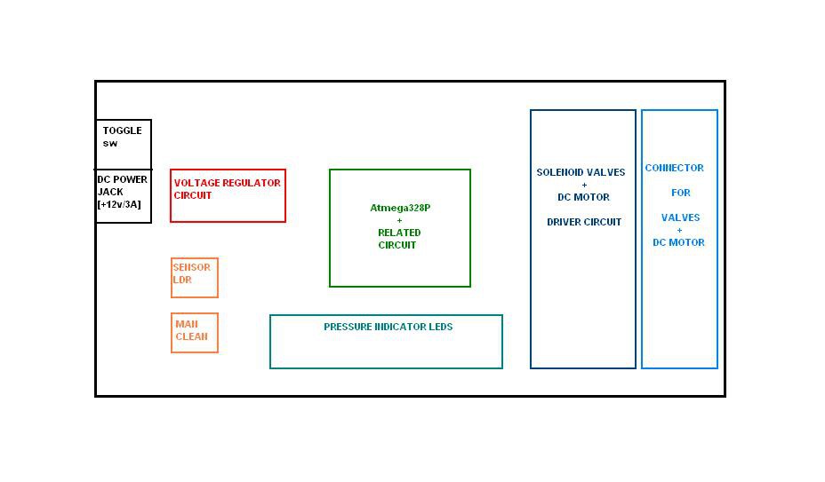
I pre-decided about the placement of the components, by considering ease of use, ease of routing, minimum noise.
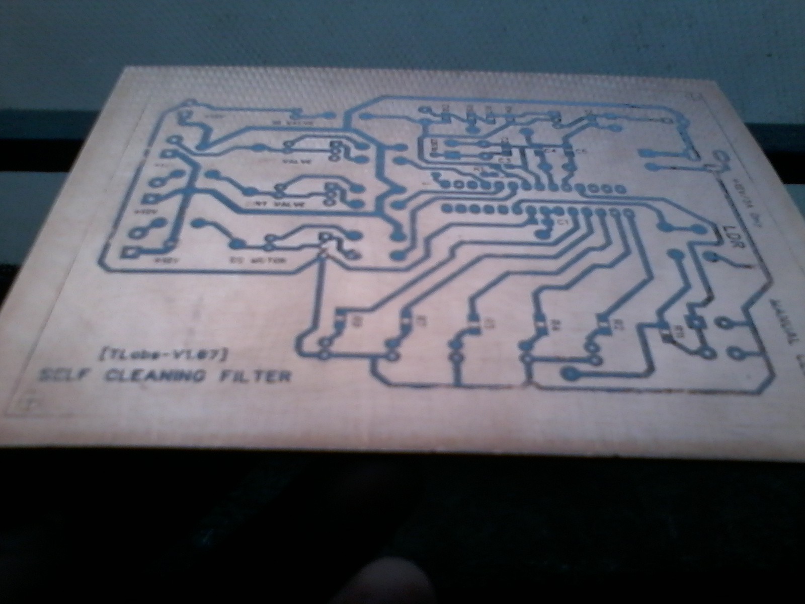
PCB will be Single Layer & Homemade, baked at college lab.
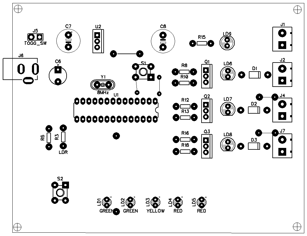
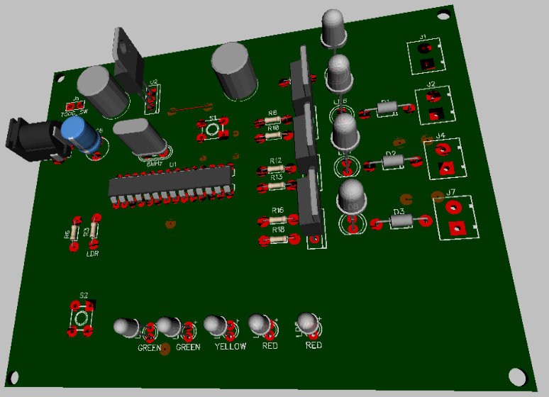
PCB design with DipTrace isn't a tough task.
Following are the images, to walk you through.
Home baked PCB etching.
- Single Layer
- etched using Layout photo print + Iron + Copper Clad + PCB etchantFeCl3

 Amar Potdar


Discussions
Become a Hackaday.io Member
Create an account to leave a comment. Already have an account? Log In.