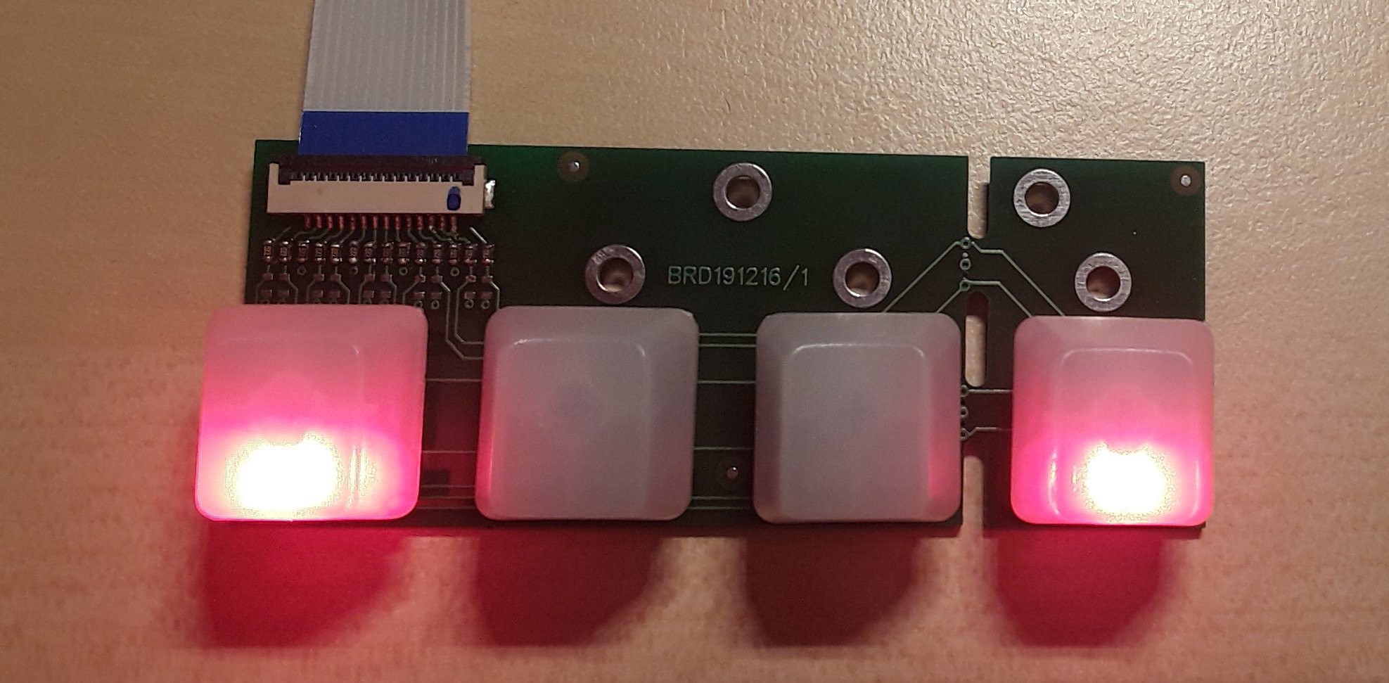
Design
The PCB has been designed using EasyEDA. You can find the design there.
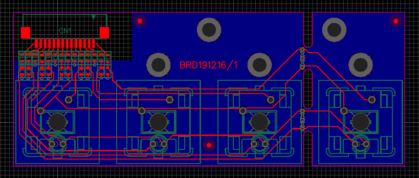
The design needed to be compact, so that multiple of these boards can be connected next to each other while keeping the same spacing between the buttons. The rightmost button can be snapped off, if needed.
EMC precautions : resistors and capacitors for filtering, ground plane for signal return. One third of the FFC pins is GND. The ground plane on the rightmost switch is poorly connected to the other ground plane. We'll see what it brings.
Component choices
Interconnection
Requirements for the connectors : cheap, small, easy to solder. Which brings to to the 1.0mm pitch FFC cable.
 | 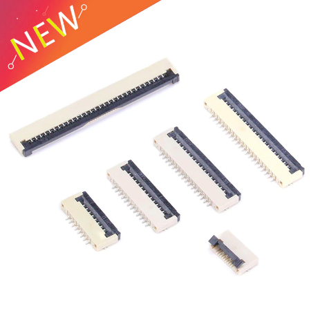 | 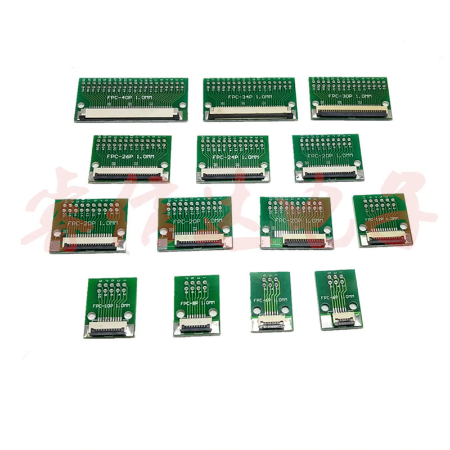 |
| A little search on AliExpress "ffc 14 pin", brings up a source that can deliver the cables for €0.10/pce. | The matching connectors can be had for about €0.05/pce. | For debugging, AliExpress also provides breakout boards at €0.91/pce. Remark that the breakout comes in dual row, so it's not breadboard friendly. |
Buttons
Requirements : big buttons, should be able to handle lots of operations, visual feedback (through LED). The selection can be found on a separate page.
Bonus facts
The I²C-expander uses matrix keyboard scanning. This requires 8 IO lines for 15 switches. If not enough IO lines had been available, there would be an alternative approach as described by Mosaic Industries:
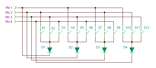
This technique would require only 5 IO lines for 15 switches (max. 20 switches). The downside is that 5 diodes need to be added. This probably won't work with an SX1509 or similar which has a built in keypad scanning engine.
 Christoph Tack
Discussions
Become a Hackaday.io Member
Create an account to leave a comment. Already have an account? Log In.